CO.,LTD")
Warum stapeln?
Die unumkehrbare Entwicklung der modernen Elektronik treibt immer mehr voran Leiterplatten gegenüber Forderungen wie der Miniaturisierung, geringes Gewicht, hohe Geschwindigkeit, bessere Funktionalität und Zuverlässigkeit, und längere Lebensdauer, was zur Beliebtheit von Multilayer-Leiterplatten führt. Kombiniert durch eine Art halbfesten Klebstoff, der genannt wird “Prepreg”, Zur Erzeugung werden zwei oder mehr ein- und/oder doppelseitige Leiterplatten gestapelt mehrschichtige Leiterplatten durch zuverlässige vordefinierte gegenseitige Verbindung zwischen ihnen. Es gibt drei oder mehr leitende Schichten in einer mehrschichtigen Leiterplatte, wobei zwei Schichten außen und eine Schicht in der Isolierplatte synthetisiert sind. Mit der Zunahme der PCB-Komplexität und -Dichte, Es ist möglich, dass einige Probleme auftreten, z. B. Lärm, Streukapazität und Übersprechen, wenn die Schichtanordnung ineffizient gestaltet wird.
Optimal planen mehrschichtiger Aufbau ist eines der wichtigsten Elemente bei der Bestimmung der elektromagnetischen Verträglichkeit (EMV) Leistung eines Produkts. Ein gut konzipierter Schichtaufbau kann sowohl die Strahlung minimieren als auch verhindern, dass der Schaltkreis durch externe Rauschquellen gestört wird. Gut gestapelte Leiterplattensubstrate können außerdem Probleme durch Signalübersprechen und Impedanzfehlanpassungen reduzieren. Jedoch, Ein minderwertiger Aufbau kann elektromagnetische Störungen verursachen (Elektromagnetische Störung) Strahlung steigt, denn Reflexionen und Nachschwingungen im System aufgrund einer Impedanzfehlanpassung können die Produkte drastisch verschlechtern’ Leistung und Zuverlässigkeit. Dieser Artikel konzentriert sich dann auf die Definition des Ebenenstapels, seine Gestaltungsregeln und wesentlichen Überlegungen.
Was ist Stack-up??
Beim Stapeln handelt es sich um die Anordnung von Kupferschichten und Isolierschichten, aus denen eine Leiterplatte besteht, bevor das Leiterplattenlayout entworfen wird. Während ein Schichtenstapel es Ihnen ermöglicht, durch die verschiedenen Schichten mehr Schaltkreise auf einer einzigen Platine unterzubringen Leiterplattenschichten, Die Struktur des PCB-Stack-Up-Designs bietet viele weitere Vorteile:
• Ein PCB-Schichtenstapel kann Ihnen helfen, die Anfälligkeit Ihrer Schaltung gegenüber externem Rauschen zu minimieren, Strahlung zu minimieren und Impedanz- und Übersprechprobleme zu reduzieren Hochgeschwindigkeits-PCB-Layouts.
• Ein guter PCB-Lagenaufbau kann Ihnen auch dabei helfen, Ihren Bedarf an niedrigen Kosten auszugleichen, effiziente Herstellungsmethoden mit Bedenken hinsichtlich Signalintegritätsproblemen
• Der richtige PCB-Lagenstapel kann auch die elektromagnetische Verträglichkeit Ihres Designs verbessern.
Für Ihre platinenbasierten Anwendungen ist es oft von Vorteil, eine gestapelte PCB-Konfiguration zu wählen.
Für mehrschichtige Leiterplatten, Zu den allgemeinen Schichten gehört die Grundebene (GND-Ebene), Kraftflugzeug (PWR-Flugzeug), und innere Signalschichten. Hier ist ein Beispielstapel eines 6-Schicht Rogers PCB.
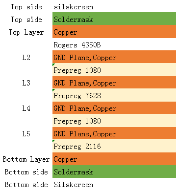
In Übereinstimmung mit dieser Abbildung, Es ist offensichtlich, dass die Schichtverteilung in Leiterplatten einer symmetrischen oder ausgewogenen Struktur entspricht. Abgesehen von der Schichtverteilung, Der Abstand zwischen den Schichten sollte ebenfalls ernst genommen werden. Um den Anforderungen der Miniaturisierung gerecht zu werden, Bei der Planung des Schichtaufbaus muss ein Mindestabstand zwischen den Leiterbahnen eingehalten werden. Der Raum zwischen den Schichten kann entweder Kern oder Prepreg sein. Mehrschichtplatten bestehen in der Regel aus mindestens einem oder mehreren Kernen und Prepregs. Die Kerne bestehen aus kupferbeschichteten, glasfaserverstärkten Epoxidlaminatplatten. Die Dicke des Kerns liegt im Bereich von 0,1 mm bis 0,3 mm.
Prepreg ist die gebräuchliche Bezeichnung für ein Verstärkungsgewebe, das mit einem Harzsystem vorimprägniert wurde. Dieses Harzsystem (typischerweise Epoxidharz) Der richtige Härter ist bereits im Lieferumfang enthalten. Die Hauptfunktion von Prepreg besteht darin, alle Schichten durch hohe Temperaturen zu einer ganzen Platte zu stapeln. Die folgende Tabelle zeigt die physikalischen und chemischen Eigenschaften der Hauptkategorien von Prepreg, das heißt, 1080,2116, Und 7628.
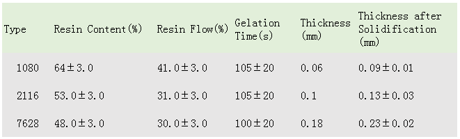
Eigentlich, Dicke jeder Art von Prepreg ist nicht immer stabil und es werden Anpassungen vorgenommen, um den spezifischen Anforderungen an die Leiterplattendicke gerecht zu werden. Bei der Bestimmung der Anzahl der Prepregs müssen einige Faktoren berücksichtigt werden, darunter die Dicke der Innenschicht, Anforderungen an die Dicke des Produktdesigns oder die Herstellung Technologiebedarf, Eigenschaften von Prepreg, praktische Leistung und die tatsächliche Dicke nach dem Stapelversuch. Also. Die gesamte Dickentoleranz der fertigen Leiterplatte beträgt ±10 %..
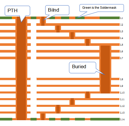
Blind Via und Buried Via Stapeln
Wenn Ihnen die Idee des PCB-Aufbaus für Ihre elektronischen Anwendungen gefällt Leiterplatten, Der einzige Ort, an den Sie für den PCB-Stack gehen müssen, ist Alcanta. Wir sind ein Komplettanbieter rund um die Leiterplatte. Wir können Ihnen helfen:
• Entwickeln Sie Ihr PCB-Stackup-Design
• Stellen Sie Ihre Schichtaufbau-PCBs her
• Erstellen Sie Prototypen, um Ihre Designs auf mögliche Fehler zu testen
• Führen Sie vollständige PCB-Durchläufe durch
Mit über zehn Jahren Erfahrung im Bereich der Leiterplattenfertigung, Sie können sicher sein, dass Alcanta ein Name ist, auf den Sie sich verlassen können mehrschichtige Leiterplatten und alle Ihre PCB-bezogenen Bedürfnisse. Wir zeichnen uns durch eine schnelle Auftragsabwicklung aus, Qualität und Wert in einem Ausmaß, das andere Hersteller von Leiterplatten nicht erreichen können. Unsere Standard-Leiterplatten erfüllen die strengen Anforderungen IPC2 und IPC3 Qualitätsstandard, und unser Unternehmen ist vollständig ISO9001:2008 konform. Bitte senden Sie eine E-Mail mit Ihren PCB-Gerber-Dateien. Bei Fragen können Sie sich gerne an unsere PCB-Ingenieure wenden.