PCB Material Selection Guide
Printed circuit board is the most important part of electronics. Alternately, the acronym has also accounted for printed wiring boards and printed wiring cards, which are essentially the same thing. Due to the crucial role of these boards in everything from computers to calculators, PCB material selection should be undertaken with care and knowledge for electrical necessities of a given piece of equipment.
Before the development of the PCB, circuit board materials were mostly covered by nests of entangled, overlapping wires that could easily fail at certain junctures. They could also short circuit once age took hold and certain wires started to crack. As could be expected, the manual process that went into the wiring of these early boards was confusing and painstaking.
As an increasing variety of everyday electronic components began to rely on circuit boards, the race was on to develop simpler, more compact alternatives, and this led to the development of the material, PCB. Cu PCB materials, circuits can be routed between a host of different components. The metal that facilitates the transfer of current between the board and any attached components is known as solder, which also serves a dual purpose with its adhesive qualities.
PCB Material Composition
PCB generally consists of four layers, which are heat laminated together into a single layer. The material used in PCB from top to bottom includes Silkscreen, Soldermask, Copper and Substrate.
The last of those layers, substrat, is made of fiberglass and is also known as FR4, with the FR letters standing for “fire retardant.” This substrate layer provides a solid foundation for PCBs, though the thickness can vary according to the uses of a given board.
A cheaper range of boards also exist on the market that don’t utilize the same aforementioned PCB materials, but instead consist of phenolics or epoxies. Due to the thermal sensitivity of these boards, they tend to lose their lamination easily. These cheaper boards are often easy to identify by the smell they give off when being soldered.
PCB second layer is copper, which is laminated onto the substrate with a mixture of heat and adhesive. The copper layer is thin, and on some boards there are two such layers – one above and one below the substrate. PCBs with only one layer of copper tend to be used for cheaper electronics devices.
Above the green soldermask is the silkscreen layer, which adds letters and numerical indicators that make a PCB readable to tech programmers. Acest, la rândul său,, makes it easier for electronics assemblers to place each PCB in the proper place and in the right direction on each component. The silkscreen layer is usually white, though colors such as red, yellow, gray and black are also sometimes used.
PCB Layer Technical Terms
Besides knowing how PCB is layered, you should know technical terms accompanies the use of PCBs:
• Annular ring. The copper ring that surrounds the holes on a PCB.
• DRC. An acronym for design rule check. În esență, DRC is a practice whereby the design of a PCB is checked for its functionality. Details that are checked include the width of the traces and drill holes.
• Drill hit. Used to describe all holes on a PCB, whether correct or misplaced. În unele cazuri, a hole might be slightly incorrect due to dull drilling equipment used during the production.
• Finger. Metal exposed along the board edge that serves as connecting points between two PCBs. Fingers are most often found on old video games and memory cards.
• Mouse bits. A PCB section overly drilled to the point where it threatens the board’s structural integrity.
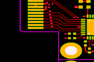
• Pad. An area of exposed metal on a PCB, onto which a soldered piece is generally applied.
• Panel. A large circuit board consisting of smaller boards, which are eventually separated for individual use.
• Paste stencil. A metal stencil on a board, onto which paste is placed for soldering.
• Plane. A larger section of exposed copper on a PCB, which is marked by borders but lacks a path.
• Plated through hole. A hole that goes straight through a PCB, usually for the purpose of connecting another component. The hole is plated and usually features an annular ring.
• Slot. Any hole that isn’t circular. PCBs with slots are often high priced due to the production costs of creating odd-shaped holes on a circuit board. Slots are typically not plated.
• Surface mount. A method whereby external parts are mounted directly to PCB without through holes.
• Trace. An ongoing line of copper across a PCB.
• V-score. A place where the board has been partially cut. This can render a PCB vulnerable to snapping.
• Via. A hole through which signals travel between layers. Tented versions are covered with protective soldermask, while the untented vias are used for connector attachments.
The number that precedes a layer refers to the exact number of conducting layers, be it a routing or plane layer – the two layer types. Layers tend to have the number 1, or any of the next four even numbers: 2, 4, 6, 8. Layer boards sometimes have odd numbers, but these are rare and would make hardly any difference. De exemplu, the PCB material in a 5 strat sau 6 layer board would be virtually identical.

The two layer types have different functions. Routing layers feature tracks. Plane layers serve as power connectors and feature copper planes. Plane layers also feature islands that determine the signaling purpose of a board, be it 3.3 V or 5 V.
 TEHNOLOGIA ALCANTA(SHENZHEN)CO., LTD