株式会社")
shdbu基板とは何ですか?
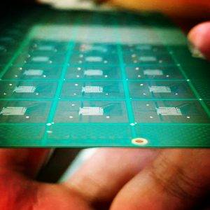
shdbu基質製造. 100umで最高のSamllestバンプピッチを作成できます, 最も小さなトレースは9umです. そして、最小のギャップは9umです. デザインのほとんどは15um〜30umのトレースと間隔です.
SHDBU基板, フルネーム超高密度の構築基板, 現在の印刷回路基板に目を引く最先端の技術です (プリント基板) 分野.
このテクノロジーの導入は、の革新的な進歩を強調しています プリント基板 エンジニアリングとメーカーに、より柔軟で強力なデザインオプションを提供します.
これらの基質の中で, 超高密度の蓄積の設計コンセプトは、回路コンポーネントの複数の層をしっかりと積み重ねることにより、優れたコンポーネント密度を実現します. これにより、より多くの電子コンポーネントを限られたスペースに統合することが可能になります, 電子製品のサイズと重量に大きな自由を提供する.
現代の電子機器におけるこれらの基質の重要な役割は、彼らが提供する優れた性能に反映されています. Shdbu基板は、電気および熱特性で優れています, 統合回路のための強固な基盤を提供します (IC) およびその他の電子部品. その高い熱伝導率により、高負荷および高周波アプリケーションでの電子デバイスの安定した動作が保証されます.
加えて, Shdbu基板は、電子製品のコンパクトな設計のための新しい可能性を提供します. この高度な基板テクノロジーにより、電子製品はパフォーマンスを損なうことなく、従来の印刷回路基板よりも小さくて軽量にすることができます.
全体, Shdbu基質の出現は、PCBエンジニアリングの分野での革命を表しています. 優れたパフォーマンスをコンパクトデザインとブレンドすることにより, この最先端のテクノロジーは、電子機器の製造における新しい開発を促進します, 将来、より高度で効率的な電子製品の基礎を築く. Shdbu基質の適用は、電子分野が絶えずイノベーションを調査している一方であることを示しています, また、製品のパフォーマンスと信頼性を常に改善しています.
SHDBU基板
Shdbu基質の機能は何ですか?
この機能は、優れた電気的および熱伝導性によって達成されます, shdbu基板を作成するのに最適なアプリケーションで最適なパフォーマンスを達成するのに最適です.
高密度設計で, Shdbu基板は際立っています, 限られたスペースに多数のコンポーネントを統合できるようにする. このプロパティは、最新の電子機器の小型化と軽量化のために重要です. 従来の基質と比較して, SHDBU基板は、超高密度スタッキング機能を通じて、電子部品をよりコンパクトで効率的な統合を実現します, デバイスのサイズと重量を最適化する可能性を提供する.
電気的な観点から, Shdbu基板の優れた性能により、信号伝達の安定性と信頼性が保証されます. これは、通信機器などのアプリケーションシナリオを要求するために重要です, 医療機器, および自律運転システム. Shdbu基質の熱伝導性も、その顕著な特徴の1つです. 現代の電子機器では, 改善された熱散逸が不可欠です, そして、Shdbu基板の設計により、限られたスペースでより効果的に熱を管理および消散させることができます.
全体, Shdbu基板は、今日の高性能に最適です, 電子成分の強固な基盤と優れた電気的および熱伝導性を提供することにより、高密度の電子デバイス設計. 統合回路やその他の主要なコンポーネントのレイアウトでのその優れたパフォーマンスは、将来の電子技術の開発に大きな影響を与えるでしょう。. PCBエンジニアリングの最先端の革新の1つとして, shdbu基板は、電子機器をより小さなものに向けて駆動するのに役立ちます, より強力でより効率的な未来.
どのような種類のShdbu基板がありますか?
PCB エンジニアリングにおいて, SHDBU基板, 革新的な開発として, 構造とパフォーマンスが異なるだけではありません, しかし、特定のアプリケーションとパフォーマンス要件に応じて複数のタイプに分けられます, 電子設計に対する柔軟性と適応性を高めることができます. セックス. 以下は、shdbu基板の一般的なタイプです:
単層shdbu
シングル層SHDBU基板は、基板構造に単純な単一層設計を備えており、スペース要件が低いアプリケーションに適していますが、パフォーマンスが高くなります。. その合理化されたデザインは、それを軽量で費用対効果の高い選択にします, 特に、柔軟性と軽量のための特別な要件がある分野で.
多層Shdbu
多層SHDBU基質は、多層積み重ねられた構造を介してより高いコンポーネント統合密度を実現するより複雑な設計です。. このタイプは、スペースが制限されているが、多数のコンポーネントを統合する必要があるアプリケーションに適しています, 高性能の電子デバイスをより強力なサポートを提供します.

SHDBU基質
ハイブリッドshdbu
ハイブリッドShdbu基板は、単一層と多層の利点を組み合わせています, 設計者により大きな自由を提供します. このタイプの基板は、柔軟性と信号の整合性要件のバランスをとりながら、高密度の要件を満たしています. ハイブリッドSHDBU基板は、柔軟性のためにさまざまなアプリケーションシナリオに適しています.
Shdbu基板の各タイプは、柔軟性の独自の利点を提供します, 信号の完全性と熱管理. 柔軟性の観点から, 彼らはさまざまな形や湾曲のデザインに適応することができます, 特別なアプリケーションに大きな自由を提供します. 信号の完全性の観点から, 高密度の積み重ねられた構造は、信号透過の電磁干渉を減らし、信号の品質を向上させるのに役立ちます. 熱管理に関して, これらのさまざまな種類のShdbu基質は、電子成分の安定した動作を確保するために、最適化された積み上げ構造を介して効果的に分散し、熱を伝導します.
全体, 多様な種類のSHDBU基板は、特定のプロジェクトのニーズとパフォーマンス要件に基づいてカスタマイズするためのより多くのオプションをエンジニアに提供します. 究極のパフォーマンスを追求するのがハイテク分野にあるかどうか, または、より高い軽量と柔軟性を必要とするフィールドで, Shdbu基板は、優れた適応性とパフォーマンスを実証しています. これにより、彼らは現代の電子デザインに不可欠な重要なテクノロジーになります.
Shdbu基板と従来のPCBの違いは何ですか?
PCBエンジニアリングの分野で, Shdbu基板は、従来の印刷された配線板と比較して人目を引く革新を提示します (PWBS) プリントサーキットボード (プリント基板). 従来のPWBとPCBは、電子デバイスの構成要素として重要な役割を果たしていますが, Shdbu基板は、独自の特性を通じて設計に大きな進歩をもたらしました.
初め, SHDBU基板は、より高いコンポーネント密度と改善された信号伝送機能を提供することにより、設計の進歩を促進します. 従来の基質と比較して, Shdbu基板には優れた積み重ね能力があります, 限られたスペースでよりコンポーネントをよりコンパクトに統合できるようにする. この技術の革新は、電子機器の設計により大きな柔軟性をもたらし、小規模の最新の電子製品のニーズをより効果的に満たすことができます, 軽量で高性能.
マザーボードのデザインに関して, Shdbu基板は、製造業者に創造性の余地を増やすことができます. この高度な基質技術を使用することにより, メーカーは、よりコンパクトで効率的なレイアウトを設計することができます, 全体的な電子デバイスの小型化に貢献します. Shdbu基板の高密度特性は、マザーボードのレイアウトオプションをより多く提供します, パフォーマンスを維持しながら、電子デバイスがサイズの要件を縮小することを容易にする.
基質様PCBと比較して (SLP), Shdbu基板には、スタッキング機能に利点があります. その類似点にもかかわらず, Shdbu基板は、より大きなスタッキング機能を提供することにより、より複雑な回路をより小さなフットプリントに統合することを可能にします. これにより、デザイナーは、電子コンポーネントのレイアウトと相互接続により、より革新的になる自由を得ることができます.
高密度の相互接続と比較してください (HDI) 基板, Shdbu基質は、技術をさらに新しい高さに押し上げます. それらは密接に関連していますが, SHDBU基板は、前例のないレベルの密度と機能を可能にすることにより、電子デバイスのパフォーマンスを大幅に向上させます. このイノベーションは、電子デバイスをよりコンパクトにするだけではありません, また、信号伝送で優れた性能を達成します, 熱管理, 等.
要約すれば, Shdbu基板は、優れた性能と高度な設計の柔軟性により、PCBエンジニアリング分野で画期的なテクノロジーになりました. コンポーネント密度と信号伝送機能を最適化します, マザーボードのデザインにユニークな貢献をしています, スタッキング機能, 等, Shdbu基板は、将来の電子機器の開発のための新しい可能性を開きます.
Shdbu基板の構造と生産技術は何ですか?
SHDBU 基板の構造は、現代のプリント基板エンジニアリングの典型的な表現です。, 単なる素材の重ね合わせを超えて、高品質なコンポーネントを巧みに応用することで実現します。. その核心, この構造は、高度な絶縁材料と導電層を複雑に積み重ねて洗練されたシステムを実現しています。.
特に, 先進的な絶縁材料の重要性は、SHDBU 基板構造の形成において最も重要です. これらの材料は、優れた断熱特性を示すだけでなく、極端な条件に対する回復力も示します。, 高温多湿を含む. この慎重な材料選択により、SHDBU 基板はさまざまな環境シナリオにわたって安定した信頼性の高い性能を維持できます。.
第二に, 導電層の選択は、SHDBU 基板の電気特性に直接影響します。. これらの導電層は、電流が構造全体に効率的に伝達され、信号損失が低減されるように、正確に設計および処理されています。. この設計は、現代の電子機器の高効率と高信頼性の要件を考慮しています。, SHDBU 基板が密なレイアウトでも優れた電気的性能を維持できるようにする.
この慎重に設計された複雑な構造は、SHDBU 基板が超高密度を実現するための重要な要素です。. 限られたスペースにより多くの電子部品を確実に収容できるよう、材料の各層の選択と配置は慎重に計算されています。, 現代の電子機器の小型化と高性能化の可能性を提供します。.
p生産技術
SHDBU 基板の製造には、いくつかの重要な製造技術が含まれます, これらの技術の継続的な革新が SHDBU 基板の開発を推進します。.
初め, 改良されたHDI製造技術 (高密度相互接続) SHDBU基板の製造の重要な部分です. 高度な製造設備とプロセスを使用することにより、, メーカーは、より微細な機能とより高い層間密度を達成できるようになります。. このテクノロジーの継続的な進歩により、SHDBU 基板はより小さな設置面積でより多くの層に対応できるようになります。, 全体的なボードパフォーマンスの向上.
第二に, 革新的なセミアディティブ法は、SHDBU 基板の製造に別の可能性をもたらします。. 従来の添加法との比較, この方法により、製造プロセスの一部のステップが削減されます, それにより製造効率が向上します. この革新的な生産技術により、メーカーは高品質と効率を維持しながら市場の需要により柔軟に対応できるようになります。.
これらの生産技術の組み合わせにより、SHDBU基板の製造を強力にサポートします。, 高密度で優れた役割を果たすことができます。, 高性能電子設計.
全体, SHDBU基板の最高峰の融合’ プリント基板工学における最先端のイノベーションを反映した構造と生産技術. この非常に複雑かつ洗練されたデザインは、現代の電子機器の発展を促進するだけでなく、, だけでなく、将来の電子技術の進歩のための強固な基盤も築くことができます。.
SHDBU基板のFAQ
SHDBU 基板と従来の基板の違いは何ですか?
SHDBU 基板は従来の基板とは大きく異なります. 従来の基板はコンポーネント密度と信号伝送に制限があります, 一方、SHDBU 基板は超高密度スタッキング技術を使用して、より多くのコンポーネントをより小さなスペースに収容します。, 全体的なパフォーマンスの向上.
SHDBU 基板は高周波アプリケーションに適していますか?
はい, SHDBU 基板は高周波用途に非常に適しています. 先進的な素材と設計により、高周波環境において優れた信号整合性が保証されます。, 複雑な回路や高周波通信の処理に最適です。.
SHDBU 基板は他の高密度基板とどう違うのか?
SHDBU 基板は、他の高密度基板と比較して、より高度な積層機能を備えています。. より小さなサイズの設計を可能にする構造と製造技術, より高度な統合, さらに複雑な回路, それにより現代の電子機器において重要な役割を果たしています.
SHDBU基板の製造技術の特徴は何ですか?
SHDBU基板の製造技術には、改良されたHDI製造技術と革新的なセミアディティブ法が含まれています. これらの技術の導入により、メーカーは電子機器の設計に対する需要の高まりに応えるため、より微細な形状とより高い製造精度を実現できるようになります。.
SHDBU基板は大規模生産に適していますか?
はい, SHDBU基板はすでに量産で広く使用されています. 製造技術の成熟度と効率性により、産業のニーズを満たす実行可能な選択肢となっています, 電子製品の信頼性と性能を確保する.