CO., LTD")
Fabricare avansată de PCB BT,Fabricare PCB BT alb și BT negru. BT PCB va fi realizat cu tehnologie avansată de producție Msap și Sap. cele mai bune cele mai mici urme/spațiere sunt 25um/25um. când folosim baza ABF. cea mai mică urmă/spațiere sunt 9um. grosimile BT sunt de la 0,06 mm la 2,0 mm. putem produce PCB-uri BT ultrasubțiri. Materialele cu valoare mare TG vor fi mai netede pentru plăcile finite. Când asamblați componentele.efectul va fi mai bun.
Materialele de rășină BT au o mecanică excelentă, termic, și proprietăți electrice. Așa că au atins o cotă de piață mare în diverse aplicații, cum ar fi pachetele de plastic IC, Chip LED, și dispozitive de înaltă frecvență, unde sunt folosite.
Materiale BT pentru Chip-LED
Acestea sunt materialele standard de facto pentru utilizarea Chip-LED. Ele excelează în reflectivitate ridicată a luminii vizibile. Şi, sunt foarte potrivite pentru lipirea sârmei datorită proprietăților sale mecanice stabile la temperaturi ridicate și rezistenței ridicate la căldură pe termen lung. În plus, sunt materiale fără halogeni.
Vizând cipuri cu materiale de substrat de dimensiuni și mai mari pentru AI și IoT, viitorul tehnologiei informației. Tehnologia electronică avansează rapid, iar tehnologia informației se află în fruntea acestei revoluții. Tehnologia mobilă puternică, cum ar fi smartphone-urile, este deja standard, iar dispozitivele purtabile sunt doar începutul erei Internetului lucrurilor (Iot) și era viitoare a inteligenței artificiale (AI). Fiecare dintre aceste tehnologii reprezintă creșteri exponențiale ale volumului și complexității procesării informațiilor care vor necesita o revoluție dramatică în tehnologia semiconductoarelor. Laminatul BT este cheia descoperirilor tehnologice care vor face aceste tehnologii viabile..
Deblocarea inovației: Evoluția tehnologiei BT PCB: În lumea electronicii, inovația este o forță motrice care remodelează continuu peisajul progresului tehnologic. Printre componentele cruciale care au asistat la o creștere remarcabilă se numără PCB-ul BT (Placă de circuit tipărită) tehnologie. Acest articol analizează complexitățile PCB BT, semnificația sa, și tendințele care îi modelează viitorul.
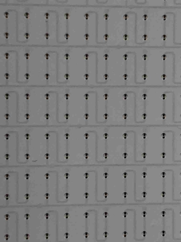
Înțelegerea tehnologiei BT PCB:PCB BT, scurt pentru “Placă de circuit imprimat cu bismaleimidă triazină,” reprezintă o clasă de substraturi de înaltă performanță utilizate în dispozitivele electronice. Aceste substraturi sunt recunoscute pentru stabilitatea lor termică excepțională, rezistenta mecanica, si performanta electrica. Fundamentul BT PCB se află în structura sa compozită, constând de obicei din straturi de țesătură de sticlă impregnate cu un sistem de rășină BT.
Una dintre caracteristicile definitorii ale tehnologiei BT PCB este capacitatea sa de a rezista la temperaturi extreme și de a oferi o platformă stabilă pentru componente electronice complexe.. Acest lucru face ca PCB-urile BT să fie potrivite pentru aplicații care necesită fiabilitate în condiții dificile, precum cele aerospațiale, auto, și industriile telecomunicațiilor.
Progrese și tendințe: Miniaturizare:Ca cererea pentru mai mici, dispozitivele electronice mai puternice cresc, PCB-urile BT au evoluat pentru a susține tendința de miniaturizare. Interconexiunile lor de mare densitate (HDI) iar factorii de formă redusi permit crearea de ansambluri electronice compacte, dar eficiente. Pe măsură ce cererea de mai mici, dispozitivele electronice mai puternice cresc, PCB-urile BT au evoluat pentru a susține tendința de miniaturizare. Interconexiunile lor de mare densitate (HDI) iar factorii de formă redusi permit crearea de ansambluri electronice compacte, dar eficiente.
Performanță de înaltă frecvență:Odată cu apariția 5G și nevoia tot mai mare de transmisie de date de mare viteză, PCB-urile BT au înregistrat îmbunătățiri ale capacităților lor de înaltă frecvență. Sunt proiectate pentru a minimiza pierderea semnalului și pentru a menține integritatea semnalului, asigurarea unei comunicări fără întreruperi în aplicațiile wireless moderne.
PCB-uri flexibile și rigide: Integrarea flexibilității în PCB-urile BT a deschis porți către noi posibilități de proiectare. PCB-urile flexibile și rigide bazate pe tehnologia BT și-au găsit aplicații în dispozitivele portabile, electronice medicale, si mai mult, datorită capacității lor de a se conforma formelor și spațiilor unice.
Considerații de mediu: Sustenabilitatea a devenit o preocupare semnificativă în toate industriile. PCB-urile BT au luat măsuri către respectarea mediului prin încorporarea materialelor cu impact mai mic asupra mediului și reciclabilitate îmbunătățită, contribuind la impulsul global pentru o tehnologie mai ecologică.
Aplicații în industrie:Aplicatiile de PCB BT tehnologiile sunt vaste și diverse: Aerospațial și Apărare: PCB-urile BT sunt parte integrantă a sistemelor aerospațiale, unde suportă temperaturi extreme și solicitări mecanice. Sunt angajați în avionică, sisteme de comunicatii, și tehnologie prin satelit. Electronică auto: În sectorul auto, PCB-urile BT acceptă sisteme avansate de asistență pentru șofer (ADAS), sisteme de infotainment, și electronica grupului de propulsie. Fiabilitatea lor asigură performanțe consistente chiar și în cele mai dure condiții de condus. Rețele de comunicații: Coloana vertebrală a rețelelor moderne de comunicații se bazează pe PCB-uri BT de înaltă performanță pentru routere, întrerupătoare, și alte echipamente de rețea. Capacitățile lor de mare viteză facilitează transferul eficient de date. Dispozitive medicale: Electronica medicală necesită precizie și fiabilitate. PCB-urile BT sunt utilizate în echipamentele de imagistică medicală, Sisteme de monitorizare a pacienților, și dispozitive implantabile, contribuind la diagnosticarea corectă și îngrijirea pacientului.
Drumul Înainte:Pe măsură ce tehnologia continuă să evolueze, PCB-urile BT vor juca probabil un rol din ce în ce mai vital în modelarea peisajului electronic. Inovații precum managementul termic îmbunătățit, materiale îmbunătățite, și sunt așteptate o miniaturizare ulterioară. Cererea de viteze mai mari de date, integrare mai mare a dispozitivului, iar responsabilitatea de mediu va ghida direcția dezvoltării viitoare a tehnologiei BT PCB. În concluzie, Tehnologia BT PCB este o dovadă a progresului ingineriei electronice. Proprietățile sale unice, împreună cu adaptabilitatea sa la tendințele emergente, poziționați-l ca un jucător cheie în realizarea dispozitivelor electronice de ultimă generație. Pe măsură ce călătorim către un viitor condus de conectivitate și eficiență, evoluția PCB-urilor BT va continua, fără îndoială, să aibă un impact profund….
Ce este Advanced BT PCB?
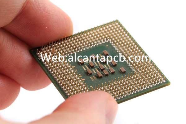
PCB BT avansat, numele complet al plăcii de circuite imprimate avansate Bismaleimid Triazine (BT) substrat, este o componentă electronică realizată din materiale de înaltă performanță. Joacă un rol vital în echipamentele electronice moderne, oferind suport de circuit de încredere și funcții de conectare pentru diverse aplicații de înaltă frecvență și viteză mare.
Principalul material utilizat în Advanced BT PCB este Bismaleimid Triazine (BT) substrat. Substraturile BT au o rezistență mecanică excelentă, rezistență termică și proprietăți electrice, făcându-le ideale pentru dispozitivele electronice de înaltă performanță. În comparație cu materialele tradiționale, Substraturile BT au o rezistență mai mare la temperaturi ridicate și pot menține proprietăți electrice stabile în medii extreme, îndeplinind astfel cerințele ridicate de fiabilitate și stabilitate ale echipamentelor electronice moderne.
În echipamente electronice, Advanced BT PCB joacă un rol cheie în conectarea și susținerea diferitelor componente electronice. Ca purtător de circuite electronice, conectează diverse componente electronice prin căi conductoare pentru a forma un circuit complet. În același timp, Advanced BT PCB poate oferi, de asemenea, suport mecanic și protecție pentru a proteja componentele electronice de mediul extern. Datorită caracteristicilor excelente de înaltă frecvență ale substratului BT, Advanced BT PCB poate fi, de asemenea, utilizat în domeniul transmisiei de mare viteză și al procesării semnalului pentru a oferi performanțe și stabilitate mai ridicate pentru echipamentele electronice.
În general, Advanced BT PCB nu este doar o componentă indispensabilă a echipamentelor electronice moderne, dar şi unul dintre motoarele importante care promovează dezvoltarea tehnologiei electronice. Materialele de înaltă performanță și performanța superioară utilizate oferă suport tehnic de încredere pentru îmbunătățirea performanței și inovarea echipamentelor electronice.
Care sunt pașii cheie în proiectarea PCB BT avansat?
Proiectarea Advanced BT PCB este o muncă complexă și precisă, iar inginerii trebuie să treacă printr-o serie de procese riguroase pentru a asigura performanța și fiabilitatea produsului final. Următorii sunt pașii cheie pentru proiectarea PCB BT avansat:
La începutul proiectării, inginerii trebuie mai întâi să lucreze cu clientul sau echipa de proiect pentru a înțelege nevoile și specificațiile tehnice ale proiectului. Ele adună și analizează funcționalitatea circuitului, cerințe de performanță, și orice constrângeri speciale care să formeze baza procesului de proiectare.
Pe baza analizei cerințelor, inginerul începe să deseneze schema schematică a circuitului. Ei conectează diverse componente electronice în funcție de funcțiile lor și efectuează analize ale circuitului pentru a se asigura că designul circuitului îndeplinește indicatorii de performanță așteptați.
În timpul etapei de selecție a componentelor, inginerii selectează dispozitivele adecvate pe baza cerințelor circuitului și a caracteristicilor componentelor disponibile. Apoi plasează aceste componente pe PCB și optimizează aspectul pentru a asigura integritatea semnalului și compatibilitatea electromagnetică.
Inginerii efectuează integritatea semnalului și interferența electromagnetică (EMI) analiza de simulare pentru a verifica dacă aspectul și designul circuitului îndeplinesc cerințele de performanță așteptate. Aceștia pot utiliza software profesional pentru a simula starea de funcționare a circuitului și pentru a detecta potențiale interferențe ale semnalului și probleme de sincronizare.
După ce se stabilește schema circuitului, inginerii încep proiectarea rutelor, adică, dirijarea firelor care conectează diverse componente electronice. Trebuie să ia în considerare lungimea căii semnalului, potrivirea impedanței și interacțiunea între semnale pentru a se asigura că aspectul respectă specificațiile de proiectare.
Optimizarea aspectului fizic este un pas critic în asigurarea performanței și fiabilității circuitului. Inginerii ajustează locațiile componentelor și căile de rutare pentru a minimiza întârzierile de transmisie a semnalului, discuții încrucișate, și pierderi de putere.
După finalizarea proiectării, inginerii vor efectua verificarea integrității și a fiabilității, inclusiv revizuirea schematică, verificarea regulilor de proiectare (RDC), inspectie electrica (ERC), etc.. De asemenea, pot efectua prototipuri și testare pentru a se asigura că proiectarea funcționează conform așteptărilor.
Prin procesul de proiectare riguros de mai sus, inginerii pot proiecta eficient PCB-uri BT avansate cu performanțe excelente, fiabilitate si stabilitate, oferind o bază solidă pentru dezvoltarea și aplicarea echipamentelor electronice.
Care sunt pașii cheie implicați în procesul de fabricație a Advanced BT PCB?
Procesul de fabricație al Advanced BT PCB este un proces complex și precis care implică mai mulți pași cheie, fiecare dintre acestea are un impact important asupra calității și performanței produsului final.
În primul rând, primul pas în fabricarea Advanced BT PCB este selectarea substratului. În această etapă, inginerii vor selecta bismaleimid triazină adecvată (BT) materialul substratului pe baza cerințelor de proiectare și a scenariilor de aplicare. Această alegere este crucială deoarece calitatea și performanța substratului afectează direct stabilitatea și fiabilitatea întregii plăci de circuite..
Urmează stratificarea și preprocesarea. În acest pas, mai multe straturi de substrat sunt stivuite împreună și sunt supuse pre-procesării necesare pentru a asigura lipirea netedă a stratului intermediar și pregătirea suprafeței. Precizia și acuratețea acestui proces afectează în mod direct progresul lin al pașilor următori și calitatea conexiunii interstrat a produsului final.
Apoi urmează pregătirea foliei de cupru și modelarea. Folia de cupru joacă un rol cheie în calea conductivă în PCB Advanced BT, deci procesul de preparare a foliei de cupru este crucial. În această etapă, inginerii vor acoperi suprafața substratului cu folie de cupru și vor folosi metode chimice pentru a modela folia de cupru pentru a forma căile conductoare și structurile de circuit necesare..
Urmează găurirea și placarea. În acest pas, inginerii folosesc o mașină de găurit pentru a găuri găurile în substratul pregătit pentru instalarea ulterioară a componentelor. Suprafața forată este apoi galvanizată pentru a îmbunătăți conectivitatea și rezistența la coroziune. Acest proces este esențial pentru acuratețea și fiabilitatea plăcii de circuite.
În sfârșit vine gravarea și inspecția finală. În această etapă, inginerii folosesc metode chimice pentru a grava porțiuni nedorite ale foliei de cupru de pe substrat, lăsând în urmă căile conductoare și structurile de circuit dorite. Apoi, placa trece printr-o inspecție finală pentru a se asigura că toți pașii procesului au fost finalizați așa cum sunt proiectați și că nu există defecte..
În general, procesul de fabricație al Advanced BT PCB implică mai multe procese complexe, iar fiecare pas are un impact important asupra calitatii si performantelor produsului final. Numai printr-un control precis al procesului și un management strict al calității putem asigura producția de produse Advanced BT PCB stabile și fiabile.
Care este analiza costului PCB Advanced BT?
Înțelegerea factorilor de cost pentru PCB Advanced BT este esențială pentru bugetarea și optimizarea costurilor de producție. Factori precum dimensiunea, complexitatea și cantitatea sunt principalii factori care afectează costul Advanced BT PCB.
În primul rând, dimensiunea este unul dintre factorii cheie care determină costul Advanced BT PCB. Dimensiunile mai mari ale PCB necesită mai multe materiale de substrat și resurse de producție, deci costurile cresc in consecinta. În plus, PCB-urile de dimensiuni mari necesită de obicei mai multe straturi pentru a găzdui circuite mai complexe, ceea ce crește și costurile de producție. Invers, Dimensiunile mai mici ale PCB-ului pot reduce costurile de material și de producție.
În al doilea rând, complexitatea PCB are, de asemenea, un impact important asupra costurilor. Proiectele complexe de circuite necesită mai multe straturi, cablaj mai dens, și procese mai avansate de implementat, care măresc costurile de producţie. De exemplu, PCB-urile cu cerințe de transmisie a semnalului de mare viteză sau interconexiuni multistrat costă de obicei mai mult decât simple PCB-uri cu un singur strat. Prin urmare, atunci când proiectați PCB BT avansat, există un compromis între complexitate și cost pentru a se asigura că produsul final atinge un echilibru între performanță și cost.
În cele din urmă, cantitatea este unul dintre factorii importanți care afectează costul Advanced BT PCB. În general vorbind, producția în masă poate reduce costul fiecărei unități de PCB, deoarece costurile fixe ale liniilor și echipamentelor de producție pot fi repartizate pe mai multe produse. Prin urmare, comenzile cu volum mare se pot bucura de costuri medii de producție mai mici, în timp ce costurile de producție în volum mic sunt relativ mari.
În concluzie, înțelegerea factorilor de cost ale PCB-urilor BT avansate este esențială pentru bugetarea și optimizarea costurilor de producție. Factori precum dimensiunea, complexitate, și cantitatea joacă un rol vital în determinarea costului PCB-urilor BT avansate, iar echipele de proiectare ar trebui să ia în considerare acești factori în timpul etapei de proiectare pentru a se asigura că cerințele de performanță sunt îndeplinite în timp ce costurile sunt controlate.
Ce materiale sunt utilizate de obicei în Advanced BT PCB?
Pe lângă utilizarea Bismaleimid Triazine (BT) Material de substrat, Advanced BT PCB utilizează adesea alte materiale cheie. Alegerea acestor materiale se bazează pe multe considerente, inclusiv cerințele de performanță, rentabilitate, mediul de aplicare și alți factori.
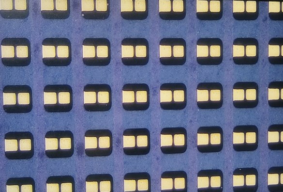
În primul rând, ca o placă de circuit imprimat de înaltă performanță, PCB BT avansat necesită de obicei materiale cu proprietăți conductoare excelente pentru a construi căi de circuit. Prin urmare, folia de cupru este un material utilizat în mod obișnuit pentru a forma căi conductoare, oferind transmisie stabilă a semnalului electric și rezistență scăzută. Folia de cupru este de obicei selectată pe baza proprietăților, cum ar fi conductivitatea sa electrică, grosime și rezistență la coroziune
În plus, ca strat protector, stratul de capac de sudură sau uleiul de capac de sudură este un material indispensabil. Stratul de capac de lipit este folosit pentru a acoperi folia de cupru pentru a o proteja de oxidarea și coroziunea mediului și pentru a oferi o suprafață lipibilă. De obicei, straturile de capac de sudură sunt selectate pentru rezistența lor la căldură, rezistență chimică, și compatibilitate cu alte materiale.
În plus, pentru a îmbunătăți rezistența mecanică și stabilitatea Advanced BT PCB, de obicei se folosesc materiale de umplutură. Aceste materiale de umplutură sunt umplute între straturile de placă pentru a spori rezistența structurală a plăcii, reduce dilatarea termică, și îmbunătățirea capacității portante a plăcii. Materialele de umplutură comune includ fibra de sticlă, Polimed (Pi), si rasina epoxidica.
Pe lângă materialele principale de mai sus, există și unele materiale auxiliare care joacă un rol important în fabricarea Advanced BT PCB. De exemplu, masca de lipit este utilizată pentru a acoperi zonele neconductoare dintre straturile de capac de lipit pentru a preveni scurtcircuitele și defecțiunile electrice. În plus, folie de cupru (Coverlay) este folosit pentru a acoperi suprafața plăcii de circuit pentru a oferi protecție și izolație suplimentară.
În general, selecția materialului PCB Advanced BT este un proces cuprinzător de luare în considerare, care trebuie să echilibreze factori precum cerințele de performanță, rentabilitatea și mediul de aplicare. Prin selectarea combinației de materiale adecvate, Advanced BT PCB poate fi asigurat că are performanțe electrice excelente, stabilitate si fiabilitate, și este potrivit pentru diferite scenarii de aplicare de înaltă frecvență și viteză mare.
Cine face Advanced BT PCB?
Producătorii joacă un rol vital atunci când explorează procesul de fabricație al Advanced BT PCB. Pentru multe companii, alegerea producătorului potrivit este un pas critic în asigurarea calității și fiabilității produsului. Pentru PCB BT avansat, producătorul însuși este o echipă de producție în cadrul unei companii.
Pentru multe companii, a avea o echipă internă de producție de PCB este una dintre cheile pentru a realiza controlul calității produselor și timpul de livrare. Pentru PCB-uri BT avansate, producătorii noștri sunt echipa de producție internă a companiei, care au o vastă experiență și expertiză pentru a se asigura că produsele îndeplinesc standardele înalte ale cerințelor de producție.
A avea o echipă de producție internă aduce multe avantaje. Primul, membrii echipei au o înțelegere profundă a produselor și tehnologiilor companiei și pot înțelege mai bine cerințele de proiectare și nevoile clienților. În al doilea rând, echipele interne de producție pot răspunde la schimbări și urgențe mai flexibil, scurtează timpii de livrare și asigură calitatea produsului. În plus, pot lucra îndeaproape cu echipa de proiectare pentru a rezolva prompt posibile probleme și pentru a îmbunătăți continuu procesul de producție.
Echipa de producție a companiei implementează procese de producție stricte pentru a se asigura că fiecare PCB Advanced BT îndeplinește standardele înalte ale companiei și ale industriei.. De la achiziția de materiale până la controlul procesului, fiecare pas este atent proiectat și executat cu strictețe. Controlul calității este o prioritate de top în timpul procesului de producție, cu inspecții și teste stricte, asigurându-se că fiecare produs îndeplinește așteptările și cerințele clienților.
Ca producator, compania noastră aderă întotdeauna la principiul clientului în primul rând. Echipa de producție nu se angajează doar să furnizeze produse de înaltă calitate, dar se concentrează și pe comunicare și cooperare cu clienții. Ei ascultă în mod activ feedback-ul clienților și își îmbunătățesc continuu produsele și serviciile pentru a-și întâlni clienții’ schimbarea nevoilor.
Ca producător de PCB BT avansat, echipa de producție internă a companiei noastre joacă un rol vital în asigurarea calității produsului, timpul de livrare si satisfactia clientului. Ele oferă clienților produse excelente Advanced BT PCB cu procese de fabricație la standarde înalte, servicii excelente pentru clienți și un spirit de îmbunătățire continuă.
Care sunt cele cinci calități ale unui serviciu excelent pentru clienți?
Într-un mediu de piață foarte competitiv, serviciul de calitate pentru clienți a devenit cheia pentru construirea unei relații puternice între companii și clienți. O echipă excelentă de servicii pentru clienți ar trebui să posede următoarele cinci calități:
O echipă de servicii pentru clienți de calitate ar trebui să răspundă nevoilor și întrebărilor clienților cu eficiență și rapiditate extreme. Aceștia ar trebui să aibă mecanisme de răspuns rapid în vigoare pentru a asigura răspunsuri imediate la întrebări sau feedback din partea clienților. Prin feedback și soluții în timp util, clienții se pot simți apreciați și îngrijiți, sporind astfel încrederea și loialitatea față de afacere.
O echipă bună de servicii pentru clienți ar trebui să fie empatică și capabilă să înțeleagă și să acorde atenție clienților’ emoții și nevoi. Ar trebui să asculte activ clienții’ pareri si sugestii, tratați clienții’ probleme și necazuri sincer, și arătați respect și grijă față de clienți. Prin construirea de conexiuni emoționale, echipele de servicii pentru clienți sunt mai capabile să răspundă nevoilor clienților și să crească satisfacția clienților.
Fiabilitatea este piatra de temelie a serviciului pentru clienți. Clienții doresc să aibă încredere în serviciul și suportul oferit de companie și să obțină ajutor și soluții de încredere atunci când întâmpină probleme. Prin urmare, o echipă de servicii pentru clienți de înaltă calitate ar trebui să se concentreze pe un înalt simț al responsabilității și credibilității, respectă întotdeauna angajamentele și angajamentele sale față de clienți, și asigură o experiență de service stabilă și de încredere.
O bună comunicare este cheia unei bune relații cu clienții. O echipă de servicii pentru clienți de calitate ar trebui să aibă abilități de comunicare clare și precise și să fie capabilă să transmită informații și să rezolve problemele în mod eficient. Ar trebui să fie buni la ascultarea clienților’ pareri si feedback, oferiți clienților informațiile și suportul necesar în timp util, asigura o comunicare buna, și evitați informațiile neclare sau neînțelegerile.
Capacitatea de rezolvare a problemelor este una dintre competențele de bază ale echipei de servicii pentru clienți. O echipă de servicii pentru clienți de înaltă calitate ar trebui să aibă capacități excelente de identificare și rezolvare a problemelor și să poată analiza și rezolva rapid și precis diverse probleme și provocări întâlnite de clienți. Aceștia ar trebui să aibă cunoștințe și experiență profesională extinse și să fie capabili să ofere soluții personalizate la diferite probleme pentru a asigura satisfacția și încrederea clienților.
Printr-o echipă de service clienți cu cele cinci caracteristici de mai sus, companiile pot satisface mai bine nevoile clienților, să stabilească o imagine de marcă bună și o reputație bună, și astfel să obțină avantaje competitive și dezvoltare durabilă.
Întrebări frecvente
Ce diferențiază PCB-urile Advanced BT de PCB-urile tradiționale?
PCB-urile BT avansate utilizează Bismaleimid Triazine (BT) Material de substrat, cunoscut pentru stabilitatea sa termică ridicată și proprietățile electrice excelente. Spre deosebire de PCB -urile tradiționale, care poate folosi materiale precum FR-4, PCB-urile BT avansate oferă performanțe superioare în aplicațiile de înaltă frecvență și de mare viteză datorită compoziției lor unice a materialului.
Ce avantaje oferă tehnologia Advanced BT PCB față de alte alternative?
Tehnologia avansată BT PCB oferă mai multe avantaje, inclusiv stabilitate termică sporită, integritate îmbunătățită a semnalului, și pierderi reduse de semnal la frecvențe înalte. În plus, Substraturile BT permit un control mai strict al impedanței și o fiabilitate mai bună, făcându-le ideale pentru aplicații solicitante precum telecomunicațiile, aerospațial, și dispozitive medicale.
Este tehnologia Advanced BT PCB potrivită pentru modele flexibile sau rigid-flex?
Da, Tehnologia avansată BT PCB poate fi adaptată pentru modele flexibile și rigid-flex. În timp ce substraturile BT sunt în mod inerent rigide, pot fi combinate cu materiale flexibile precum poliimida pentru a crea PCB-uri flexibile sau configurații rigid-flex. Această versatilitate face ca tehnologia Advanced BT PCB să fie potrivită pentru o gamă largă de cerințe de proiectare.
Ce factori influențează costul de fabricație a PCB-urilor BT avansate?
Costul de fabricație a PCB-urilor BT avansate depinde de mai mulți factori, inclusiv dimensiunea plăcii, complexitate, numărul de straturi, Material de substrat, și volumul de producție. În general, număr mai mare de straturi, materiale specializate, iar producția mai mică contribuie la creșterea costurilor de producție. Cu toate acestea, optimizarea designului pentru fabricabilitate și selectarea materialelor rentabile pot ajuta la atenuarea cheltuielilor.
Dacă aveți întrebări. te rog trimite email la: Info@alcantapcb.com
Vă vom ajuta oricând. Mulţumesc mult.