CO., LTD")
Mtengenezaji wa Kifurushi cha Ajinomoto GL102R8HF.Mtengenezaji wa Kifurushi cha Kifurushi cha Ajinomoto GL102R8HF anataalamu wa kutengeneza vijisehemu vya ubora wa juu vya vifaa vya kielektroniki.. Na teknolojia ya hali ya juu na utaalamu, wanahakikisha usahihi, kuegemea, na utendaji katika bidhaa zao, kukidhi mahitaji yanayohitajika ya utengenezaji wa kisasa wa vifaa vya elektroniki.
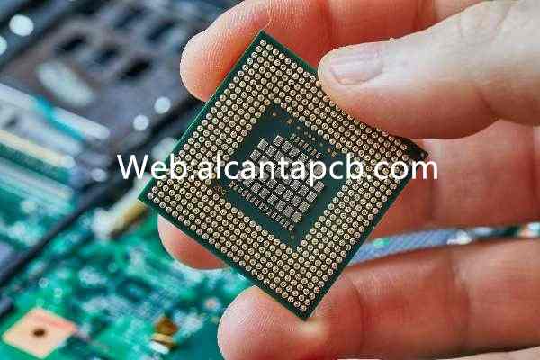
Kifurushi Kidogo cha Ajinomoto GL102R8HF ni nini?
Ajinomoto GL102R8HF substrate ya kifurushi ni nyenzo ya utendaji wa juu ya PCB iliyoundwa kwa matumizi ya elektroniki katika mazingira ya mzunguko wa juu na joto la juu.. Imetengenezwa na Kundi maarufu la Ajinomoto, substrate inajulikana kwa utendaji bora wa umeme na uwezo wa usimamizi wa joto, na ina uwezo wa kukidhi mahitaji magumu ya kuegemea juu na utendakazi wa bidhaa za kisasa za kielektroniki.
Katika kubuni na kutengeneza bidhaa za elektroniki, uteuzi wa nyenzo za substrate ya ufungaji ni muhimu. Sehemu ndogo ya ufungaji ya Ajinomoto GL102R8HF inachukua teknolojia ya hali ya juu na ina sifa ya upotezaji wa chini wa dielectric na upotezaji wa chini wa dielectric.. Sifa hizi huifanya ifanye vizuri hasa katika upitishaji wa mawimbi ya kasi ya juu, ambayo inaweza kupunguza kwa ufanisi upunguzaji wa ishara na upotoshaji na kuhakikisha utendakazi thabiti wa vifaa vya elektroniki katika mazingira ya masafa ya juu..
Aidha, kifurushi cha Ajinomoto GL102R8HF kina uwezo bora wa usimamizi wa joto. Mara nyingi umeme wa kisasa unahitaji kushughulikia kiasi kikubwa cha joto, hasa katika miundo ya mzunguko wa juu-nguvu na wa juu-wiani. Conductivity ya juu ya mafuta ya substrate inaweza kuondokana na joto haraka na kuzuia kushindwa kwa vifaa kutokana na overheating, hivyo kuboresha uaminifu na maisha ya huduma ya bidhaa za elektroniki.
Ajinomoto GL102R8HF substrate ya ufungaji sio tu ina faida katika utendaji, lakini nyenzo yenyewe pia ina kiwango cha juu cha nguvu za mitambo na upinzani wa kutu wa kemikali. Hii ina maana kwamba substrate inaweza kudumisha uadilifu wake wa kimuundo na utulivu wa kazi katika uso wa matatizo ya mitambo na hali mbaya ya mazingira.. Tabia hii hufanya sehemu ndogo ya upakiaji ya Ajinomoto GL102R8HF kutumika sana katika nyanja zinazohitaji kuegemea juu sana., kama vile umeme wa magari, Anga, na vifaa vya matibabu.
Aidha, Sehemu ndogo ya ufungaji ya Ajinomoto GL102R8HF pia ina usindikaji mzuri na uwezo wa kubadilika.. Ikiwa ni teknolojia ya kuweka uso (Smt) au miundo changamano ya PCB za tabaka nyingi, substrate hii inaweza kubadilika na kuwaunga mkono vizuri, kuwapa wabunifu wa kielektroniki uhuru zaidi wa kubuni na kubadilika.
Kwa jumla, Sehemu ndogo ya ufungaji ya Ajinomoto GL102R8HF hutoa suluhisho bora kwa matumizi ya masafa ya juu na joto la juu katika bidhaa za kisasa za elektroniki na utendaji wake bora wa umeme., uwezo wa usimamizi wa joto, nguvu ya mitambo na upinzani wa kemikali. Sio tu inaboresha utendaji wa jumla na uaminifu wa vifaa vya elektroniki, lakini pia inakuza maendeleo na maendeleo endelevu ya teknolojia katika tasnia ya umeme. Kwa kuchagua substrate ya ufungaji ya Ajinomoto GL102R8HF, wabunifu na wahandisi wa kielektroniki wanaweza kubuni na kutengeneza bidhaa za kielektroniki zenye ufanisi zaidi na zinazotegemeka ili kukidhi mahitaji ya soko yanayokua.
Mwongozo wa Marejeleo wa Usanifu wa Kifurushi cha Ajinomoto GL102R8HF.
Kifurushi cha Ajinomoto GL102R8HF ni nyenzo ya utendaji wa juu ya PCB iliyoundwa kwa matumizi ya elektroniki katika mazingira ya masafa ya juu na joto la juu.. Mwongozo huu wa marejeleo ya muundo unakusudiwa kuwapa wahandisi na wabunifu miongozo na mbinu bora za muundo wa kifurushi cha Ajinomoto GL102R8HF..
Sehemu ndogo ya ufungaji ya Ajinomoto GL102R8HF ina utendaji bora wa umeme na uwezo wa usimamizi wa mafuta., na inafaa kwa uwasilishaji wa mawimbi ya kasi ya juu na matumizi ya kielektroniki katika mazingira ya halijoto ya juu. Tabia yake ya chini ya dielectric ya mara kwa mara na ya chini ya kupoteza dielectric huhakikisha uhamisho wa ishara imara, wakati conductivity yake bora ya mafuta husaidia kufuta joto kwa ufanisi na kuhakikisha utulivu wa mfumo.
Muundo wa mpangilio: Muundo unaofaa wa mpangilio unaweza kupunguza uingiliaji wa mawimbi na mionzi ya sumakuumeme na kuboresha uwezo wa kuzuia mwingiliano wa mfumo..
Uwekaji wa sehemu: Panga vipengele ipasavyo kulingana na kazi ya mzunguko na usambazaji wa joto ili kuhakikisha usimamizi mzuri wa joto na uadilifu wa ishara.
Upana wa risasi na nafasi: Kulingana na frequency ya ishara na mahitaji ya sasa, kuamua upana wa risasi na nafasi ili kupunguza upotezaji wa upitishaji wa mawimbi na mazungumzo.
Ndege za chini na za nguvu: Sanifu ipasavyo ardhi na ndege za umeme ili kutoa ardhi thabiti na mwongozo wa nguvu na kupunguza kelele za mfumo na kushuka kwa voltage..
Chagua programu ya kitaalamu ya kubuni ya PCB na zana zinazofaa kwa muundo wa kifurushi cha Ajinomoto GL102R8HF, kama vile mbuni wa Altium, Cadence Allegro, nk., ili kuhakikisha usahihi na uaminifu wa kubuni.
Kwa matukio maalum ya maombi, kama vile upitishaji wa mawimbi ya kasi ya juu, masafa ya redio ya masafa ya juu, na mazingira ya joto la juu, tahadhari maalum inahitaji kulipwa kwa mahitaji ya kubuni katika uadilifu wa ishara, kulinganisha kwa impedance, na usimamizi wa mafuta ili kuhakikisha utendaji wa mfumo na kuegemea.
Baada ya kubuni kukamilika, udhibiti mkali wa ubora na upimaji unafanywa, ikiwa ni pamoja na ukaguzi wa malighafi, udhibiti wa mchakato wa utengenezaji na upimaji wa mwisho wa bidhaa, ili kuhakikisha kuwa bidhaa inakidhi vipimo vya muundo na mahitaji ya utendaji.
Mwongozo wa kumbukumbu ya muundo wa kifurushi cha Ajinomoto GL102R8HF umeundwa kusaidia wahandisi na wabunifu kubuni mifumo thabiti na ya kuaminika ya kielektroniki katika mazingira ya masafa ya juu na joto la juu.. Kwa kufuata kanuni za muundo na mazoea bora, faida za utendakazi wa kifungashio cha Ajinomoto GL102R8HF zinaweza kuboreshwa ili kukidhi mahitaji ya hali tofauti za utumaji..
Ni nyenzo gani inatumika katika Kifungu Kidogo cha Kifurushi cha Ajinomoto GL102R8HF?
Sehemu ndogo ya upakiaji ya Ajinomoto GL102R8HF hutumia masafa ya juu na nyenzo za uthabiti wa hali ya juu., ambayo hutoa msingi wa kuaminika wa utendaji wa bidhaa za kisasa za elektroniki. Vipengele vyake muhimu ni pamoja na hasara ya chini ya dielectric na hasara ya chini ya dielectric, ambayo inaruhusu kufanya vizuri katika maambukizi ya kasi ya kasi na mazingira ya joto la juu. Katika bidhaa za elektroniki, kasi na utulivu wa maambukizi ya ishara ni muhimu, na kiwango cha chini cha dielectric cha Ajinomoto GL102R8HF huhakikisha uthabiti wa upitishaji wa ishara na kupunguza uwezekano wa kupunguza na kupotosha kwa ishara., hivyo kuboresha uaminifu na utendaji wa mfumo.
Aidha, Nyenzo ya Ajinomoto GL102R8HF ina nguvu bora ya mitambo na upinzani wa kemikali. Katika matumizi ya vitendo, bidhaa za kielektroniki zinaweza kuathiriwa na mambo kama vile mtetemo wa kimitambo, athari, au kutu kwa kemikali katika mazingira. Tabia bora za mitambo na upinzani wa kutu wa nyenzo hii inaweza kulinda kwa ufanisi muundo wa ndani na vipengele vya mzunguko wa substrate ya ufungaji.. Hakikisha utendakazi wake thabiti wa muda mrefu.
Kwa jumla, Nyenzo ndogo ya ufungaji ya Ajinomoto GL102R8HF ina jukumu muhimu katika bidhaa za kisasa za elektroniki kwa sababu ya utendaji wake bora wa umeme., nguvu ya mitambo na upinzani wa kutu. Utendaji wake thabiti na wa kuaminika hutoa msingi wa kuaminika kwa matumizi anuwai ya elektroniki, na pia hutoa usaidizi muhimu kwa utendaji wa juu na uaminifu wa juu wa bidhaa za elektroniki.
Sehemu ndogo ya Kifurushi cha Ajinomoto GL102R8HF ni ya ukubwa gani?
Saizi ya sehemu ndogo ya kifurushi cha Ajinomoto GL102R8HF ni muhimu kwani huamua ufaafu na utendakazi wa substrate katika vifaa mbalimbali vya kielektroniki.. Sehemu ndogo hii inaweza kubinafsishwa sana na inaweza kutengenezwa kwa usahihi na kutengenezwa kulingana na mahitaji maalum ya programu.
Kwa vifaa vya elektroniki vya watumiaji wadogo, kama vile simu mahiri, vidonge, na vifaa vya sauti vinavyobebeka, saizi ya kifurushi cha Ajinomoto GL102R8HF kwa kawaida ni ndogo. Vifaa hivi vinahitaji miundo thabiti ili kuokoa nafasi na mara nyingi huwa na vikwazo vikali vya ukubwa. Kwa hiyo, substrate ya Ajinomoto GL102R8HF inaweza kubinafsishwa kulingana na mahitaji ya saizi ya vifaa hivi., kuhakikisha kwamba inaweza kuunganishwa kikamilifu kwenye kifaa na kufikia miunganisho nzuri ya mzunguko na maambukizi ya ishara.
Kwa vifaa vikubwa vya viwandani, kama vile mifumo ya udhibiti wa viwanda, vituo vya msingi vya mawasiliano na vifaa vya anga, saizi ya kifurushi cha Ajinomoto GL102R8HF inaweza kuwa kubwa zaidi. Vifaa hivi kawaida huhitaji kushughulikia mizunguko na ishara zaidi, inayohitaji substrates kubwa zaidi ili kushughulikia vipengele hivi. Aidha, vifaa vya viwandani kawaida huhitaji kuegemea zaidi na uimara, kwa hivyo substrate ya Ajinomoto GL102R8HF pia inaweza kubinafsishwa kulingana na mahitaji haya ili kuhakikisha kuwa inaweza kufanya kazi kwa utulivu katika mazingira magumu ya kufanya kazi..
Kwa kifupi, saizi ya kifurushi cha Ajinomoto GL102R8HF inaweza kubinafsishwa kulingana na mahitaji maalum ya programu.. Ikiwa ni vifaa vya elektroniki vya watumiaji wadogo au vifaa vikubwa vya viwandani, substrates ya ukubwa sambamba inaweza kutumika. Ubinafsishaji huu hufanya substrate ya Ajinomoto GL102R8HF kuwa chaguo bora kwa vifaa anuwai vya kielektroniki., uwezo wa kukidhi mahitaji ya muundo na utendaji wa vifaa tofauti.
Mchakato wa Mtengenezaji wa Kifurushi Kidogo cha Ajinomoto GL102R8HF.
Mchakato wa utengenezaji wa kifurushi cha Ajinomoto GL102R8HF ni mchakato mgumu na sahihi unaohusisha hatua nyingi muhimu ili kuhakikisha utendaji wa juu na kutegemewa kwa bidhaa ya mwisho.. Yafuatayo ni yaliyomo kuu ya mchakato wa utengenezaji:
Hatua ya kwanza katika mchakato wa utengenezaji ni kuandaa vifaa vinavyohitajika kwa substrate ya kifurushi cha Ajinomoto GL102R8HF.. Hii ni pamoja na nyenzo za msingi za substrate, ambayo ni nyenzo ya Ajinomoto GL102R8HF, na foil ya shaba inayotumiwa kuchapisha mifumo ya mzunguko.
Uchoraji wa muundo wa shaba ni moja wapo ya hatua muhimu katika mchakato wa utengenezaji. Kwanza, safu ya foil ya shaba imewekwa juu ya uso wa substrate ya Ajinomoto GL102R8HF., na kisha etching kemikali au mbinu mitambo ni kutumika kuondoa ziada shaba foil, Kuacha muundo wa mzunguko unaotaka. Mifumo hii ya saketi itakuwa njia za uunganisho za vipengee vya kielektroniki vya siku zijazo.
Baada ya kuchora muundo wa shaba kukamilika, hatua inayofuata ni matumizi ya teknolojia ya mlima wa uso (Smt). Hii ni teknolojia ya juu ya mkutano ambayo inatambua uunganisho wa vipengele kwa vipengele vya uso wa kulehemu moja kwa moja, kama vile chips, wapinzani, capacitors, nk., juu ya uso wa substrate. Teknolojia hii inawezesha mpangilio wa sehemu ya juu-wiani na inaboresha ufanisi wa mkutano.
Kifurushi cha Ajinomoto GL102R8HF kawaida hutumia teknolojia ya utengenezaji wa PCB ya safu nyingi. Hii ina maana kwamba ndani ya substrate moja, kuna tabaka nyingi za mzunguko zilizowekwa juu ya kila mmoja, na vias au viunganisho vya ndani vya umeme vinavyounganisha saketi kati ya tabaka tofauti. Ubunifu huu huwezesha mipangilio ngumu zaidi ya mzunguko na inaboresha ujumuishaji wa mzunguko na utendaji.
Katika hatua ya mwisho ya mchakato wa utengenezaji, ni muhimu kufanya upimaji mkali wa ubora kwenye substrate ya kifurushi cha Ajinomoto GL102R8HF. Hii inajumuisha kupima uunganisho wa mzunguko, ubora wa kulehemu, utendaji wa insulation na ukaguzi wa kuona. Kupitia vipimo hivi, unaweza kuhakikisha kuwa sehemu ndogo ya ufungaji inayozalishwa inakidhi vipimo vya muundo na ina utendakazi thabiti na kutegemewa..
Kukamilisha, mchakato wa utengenezaji wa substrate ya ufungaji ya Ajinomoto GL102R8HF inahusisha hatua nyingi muhimu., ikiwa ni pamoja na maandalizi ya nyenzo, etching ya muundo wa shaba, teknolojia ya kuweka uso na teknolojia ya utengenezaji wa tabaka nyingi za PCB. Utumiaji wa teknolojia hizi huhakikisha wiani mkubwa na uaminifu mkubwa wa muundo wa mzunguko, kuifanya Ajinomoto GL102R8HF kuwa chaguo bora kwa bidhaa za kisasa za kielektroniki.
Eneo la Maombi la Kifurushi Kidogo cha Ajinomoto GL102R8HF.
Kama nyenzo ya utendaji wa juu wa PCB, Sehemu ndogo ya ufungaji ya Ajinomoto GL102R8HF inatumika sana katika nyanja nyingi.. Yafuatayo ni maeneo yake kuu ya maombi:
Katika uwanja wa matumizi ya umeme, Sehemu ndogo za ufungaji za Ajinomoto GL102R8HF hutumiwa sana katika bidhaa kama vile simu mahiri., vidonge, kompyuta za kibinafsi, na vifaa vya nyumbani. Utendaji wake wa masafa ya juu na uwezo bora wa usimamizi wa mafuta huiwezesha kukidhi kasi ya juu, mahitaji ya joto la juu na kuegemea kwa umeme wa watumiaji.
Kwenye uwanja wa umeme wa magari, Sehemu ndogo za ufungashaji za Ajinomoto GL102R8HF hutumiwa kutengeneza vifaa muhimu kama vile vitengo vya kudhibiti kielektroniki vya magari. (Funika), mifumo ya infotainment ya gari, na mifumo ya urambazaji ya gari. Kuegemea kwake juu na upinzani wa joto la juu huhakikisha uendeshaji thabiti wa mifumo ya elektroniki ya magari katika mazingira magumu.
Katika uwanja wa anga, Sehemu ndogo za ufungaji za Ajinomoto GL102R8HF hutumika katika vifaa muhimu kama vile vifaa vya avionics., mifumo ya udhibiti wa ndege, na vifaa vya mawasiliano. Tabia zake za juu za utendaji na upinzani wa joto la juu huiwezesha kukidhi mahitaji magumu ya kasi ya juu, joto la juu na kuegemea juu katika tasnia ya anga.
Katika uwanja wa vifaa vya matibabu, Sehemu ndogo za ufungashaji za Ajinomoto GL102R8HF hutumiwa kutengeneza vifaa muhimu kama vile vifaa vya upigaji picha vya matibabu., vidhibiti moyo, na mifumo ya ufuatiliaji wa matibabu. Sifa zake za utendakazi wa hali ya juu na utendakazi thabiti huhakikisha kutegemewa na usalama wa vifaa vya matibabu katika maombi ya kimatibabu.
Katika uwanja wa mawasiliano ya simu, Sehemu ndogo ya upakiaji ya Ajinomoto GL102R8HF inatumika katika vifaa muhimu kama vile vituo vya msingi vya mawasiliano., vifaa vya mawasiliano ya nyuzi za macho, na ruta za mtandao. Utendaji wake wa masafa ya juu na sifa bora za upitishaji wa mawimbi huiwezesha kukidhi mahitaji ya mawasiliano ya kasi ya juu na ya masafa ya juu katika uwanja wa mawasiliano..
Katika uwanja wa automatisering ya viwanda, Sehemu ndogo za ufungaji za Ajinomoto GL102R8HF hutumika kutengeneza vifaa muhimu kama vile roboti za viwandani., mifumo ya udhibiti wa otomatiki, na vifaa mahiri vya kiwandani. Kuegemea kwake juu na uimara huhakikisha utendakazi thabiti na kuegemea kwa muda mrefu kwa vifaa vya otomatiki vya viwandani katika mazingira ya uzalishaji..
Kukamilisha, Sehemu ndogo ya ufungaji ya Ajinomoto GL102R8HF imekuwa chaguo bora kwa kasi ya juu., maombi ya joto la juu na ya kuaminika katika nyanja nyingi na sifa zake za utendaji wa juu, kutoa msaada mkubwa na dhamana kwa maendeleo na maendeleo ya bidhaa za kisasa za kielektroniki.
Je, ni faida gani za Kifungu Kidogo cha Kifurushi cha Ajinomoto GL102R8HF?
Kama nyenzo ya hali ya juu ya PCB, Sehemu ndogo ya ufungaji ya Ajinomoto GL102R8HF ina faida nyingi na inatoa msaada muhimu kwa muundo na utendaji wa bidhaa za kisasa za kielektroniki..
Sehemu ndogo ya kifurushi cha Ajinomoto GL102R8HF imetengenezwa kwa nyenzo zilizo na upotezaji wa chini wa dielectric na upotezaji wa chini wa dielectric., kuhakikisha utendaji bora wa masafa ya juu. Katika maombi ya maambukizi ya kasi ya juu, inaweza kutoa upitishaji wa mawimbi thabiti na upitishaji data sahihi, kusaidia kudumisha utendaji wa juu na utulivu wa mfumo.
Substrate ya mfuko ina conductivity bora ya mafuta, ambayo inaweza kusambaza joto kwa ufanisi na kupunguza joto la mfumo. Katika mazingira ya joto la juu, inaweza kudumisha utulivu na uaminifu wa vipengele vya elektroniki, kupunguza matatizo ya utendaji na hatari za kushindwa zinazosababishwa na overheating, na kupanua maisha ya huduma ya vifaa.
Sehemu ndogo ya ufungaji ya Ajinomoto GL102R8HF ina nguvu bora ya mitambo na upinzani wa kutu wa kemikali., na inaweza kudumisha utulivu katika mazingira magumu ya kazi. Utendaji wake thabiti wa umeme na uimara huifanya kuwa bora kwa matumizi anuwai ya kuegemea juu kama vile anga., Vifaa vya matibabu, na mifumo ya udhibiti wa viwanda.
Sehemu ndogo za kifurushi cha Ajinomoto GL102R8HF zinaweza kubinafsishwa kulingana na mahitaji maalum ya programu, ikiwa ni pamoja na ukubwa, muundo wa safu, na mali ya nyenzo. Unyumbulifu huu huifanya kufaa kwa miundo tofauti tofauti ya bidhaa za kielektroniki na inaweza kukidhi mahitaji maalum ya tasnia tofauti na maeneo ya matumizi..
Kama nyenzo ya utendaji wa juu, Sehemu ndogo ya ufungaji ya Ajinomoto GL102R8HF inakidhi mahitaji ya mazingira, na nyenzo na michakato ya utengenezaji inayotumika inazingatia urafiki wa mazingira. Hii husaidia kupunguza athari za kimazingira za bidhaa na inaendana na mahitaji ya jamii ya kisasa ya maendeleo endelevu.
Kwa kifupi, Sehemu ndogo ya ufungaji ya Ajinomoto GL102R8HF imekuwa sehemu ya lazima na muhimu katika muundo wa kisasa wa bidhaa za elektroniki kwa sababu ya utendaji wake wa masafa ya juu., uwezo bora wa usimamizi wa mafuta, kuegemea juu, ubinafsishaji rahisi na faida za ulinzi wa mazingira. Inatoa msingi imara kwa ajili ya maendeleo na uvumbuzi wa sekta ya umeme, kusaidia maendeleo ya kiteknolojia na uboreshaji wa bidhaa katika nyanja mbalimbali za matumizi.
Maswali
Kuna tofauti gani kati ya sehemu ndogo ya kifurushi cha Ajinomoto GL102R8HF na nyenzo za jadi za PCB?
Sehemu ndogo ya upakiaji ya Ajinomoto GL102R8HF ina utendaji bora wa masafa ya juu na uwezo wa usimamizi wa mafuta kuliko nyenzo za jadi za PCB.. Imetengenezwa kwa masafa ya juu, nyenzo za utulivu wa juu wa mafuta, ina sifa ya hasara ya chini ya dielectric mara kwa mara na ya chini ya dielectric, na inafaa kwa upitishaji wa mawimbi ya kasi ya juu na matumizi ya kielektroniki katika mazingira ya joto la juu.
Jinsi ya kuchagua nyenzo zinazofaa za ufungaji?
Wakati wa kuchagua vifaa vya ufungaji wa ufungaji, mazingira ya maombi, mahitaji ya utendaji wa umeme, na usimamizi wa joto unahitaji kuzingatiwa. Ikiwa operesheni katika mzunguko wa juu au mazingira ya juu ya joto inahitajika, substrate ya kifurushi cha Ajinomoto GL102R8HF itakuwa chaguo bora kwani inatoa utendaji bora wa masafa ya juu na uwezo wa usimamizi wa mafuta..
Je, ni mambo gani ya gharama ya substrate ya kifurushi cha Ajinomoto GL102R8HF?
Gharama ya substrate ya ufungaji ya Ajinomoto GL102R8HF inategemea mambo mengi., ikiwa ni pamoja na mali ya nyenzo, utata wa mchakato wa utengenezaji, na mahitaji ya ubinafsishaji. Kwa ujumla, kutokana na utendaji wake bora na ubora wa juu, gharama ya substrate ya ufungaji ya Ajinomoto GL102R8HF inaweza kuwa juu kidogo kuliko vifaa vya jadi vya PCB., lakini faida za utendaji na kutegemewa inazoleta zitastahili pesa.
Je, ni masuala gani ya mazingira kwa ajili ya uzalishaji na utunzaji wa PCB?
Wakati wa uzalishaji na usindikaji wa PCBs, ulinzi wa mazingira wa vifaa na utupaji wa taka za uzalishaji unahitaji kuzingatiwa ili kuhakikisha kufuata kanuni za mazingira. Sehemu ndogo ya ufungaji ya Ajinomoto GL102R8HF imetengenezwa kwa nyenzo rafiki kwa mazingira na inalenga katika kupunguza taka wakati wa mchakato wa uzalishaji ili kuhakikisha athari ndogo kwa mazingira..