CO., LTD")
Cavitate PCB | Frecvență înaltă PCB fabricatie. PCB-urile cu cavitate realizate cu materiale de bază de înaltă frecvență. ca: material Rogers. sau alte tipuri Material de mare viteză. ca: Material Panasonic M7. am făcut PCB-ul din cavitate 4 strat la 50 straturi.
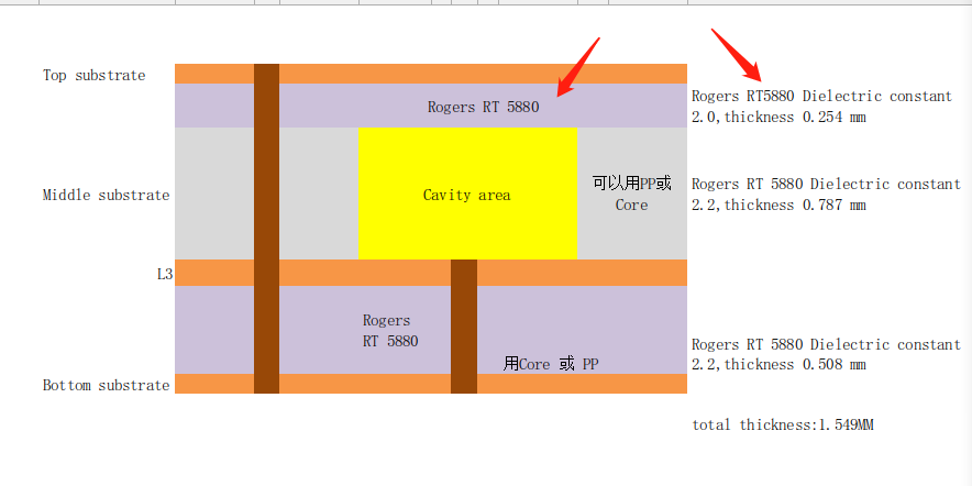
Cavity PCB este o placă de circuit imprimat special proiectată, cu o cavitate internă sau o structură cu caneluri. Caracteristicile sale de bază includ formarea de cavități pe suprafață sau în interiorul plăcii pentru a oferi un spațiu mai mare pentru componente sau pentru a îndeplini nevoi funcționale specifice. În echipamente electronice, Cavitatea PCB joacă un rol cheie, oferind o integrare mai mare, compatibilitate electromagnetică mai bună și performanță superioară de disipare a căldurii. Oferind un suport mai solid și un mediu mai potrivit pentru componentele electronice, Cavity PCB poate îmbunătăți performanța și fiabilitatea echipamentelor și poate satisface nevoile diferitelor domenii.
Cum să proiectezi Cavitate PCB?
Proiectarea unui PCB cu cavitate necesită luarea în considerare a unei serii de principii și pași cheie pentru a asigura performanța acestuia, fiabilitatea și fezabilitatea producției. Iată câteva aspecte importante de reținut atunci când proiectați Cavity PCB:
Design cavitate: Când proiectați Cavity PCB, mai întâi trebuie să luați în considerare forma, dimensiunea și locația cavității. Designul cavității trebuie să îndeplinească cerințele de aspect și conectare ale componentelor electronice, asigurându-se totodată că cavitatea este solidă din punct de vedere structural și capabilă să reziste la efectele mediului extern.
Integritatea semnalului: Proiectarea PCB-ului cavității ar trebui să ia în considerare integritatea semnalului pentru a asigura transmisia semnalului și controlul interferențelor electromagnetice în și în jurul cavității. Proiectați corect căile de semnal, fire de împământare și structuri de ecranare pentru a reduce distorsiunea semnalului și diafonia.
Managementul termic: Luarea în considerare a managementului termic în interiorul cavității este unul dintre considerentele importante în proiectarea Cavity PCB. Proiectați corect structura de disipare a căldurii și orificiile de ventilație pentru a vă asigura că componentele electronice mențin temperaturi corespunzătoare în timpul lucrului și pentru a evita deteriorarea prin supraîncălzire.
Selectarea materialelor: Alegerea materialului de substrat adecvat este crucială pentru proiectarea Cavity PCB. Materialele trebuie să aibă o conductivitate termică bună, constantă dielectrică și rezistență mecanică pentru a îndeplini cerințele aplicației specifice.
Fezabilitatea producției: Când proiectați Cavity PCB, trebuie luată în considerare fezabilitatea fabricării acestuia. Evitați proiectarea unor structuri prea complexe sau irealizabile și asigurați-vă că designul poate fi transformat fără probleme în procesul de producție real.
Ambalare și Asamblare: În cele din urmă, procesul de ambalare și asamblare trebuie luat în considerare la proiectarea PCB-ului Cavity. Alegeți metoda de ambalare adecvată pentru a vă asigura că componentele electronice sunt fixate în siguranță în cavitate și pot fi asamblate și testate cu succes ulterior.
În concluzie, proiectarea Cavity PCB necesită o analiză cuprinzătoare a designului cavității, integritatea semnalului, management termic, Selectarea materialelor, fezabilitatea fabricației și asamblarea ambalajului. Doar luând în considerare pe deplin acești factori, un PCB cu cavitate poate avea performanțe excelente, fiabilitatea și stabilitatea să fie proiectate pentru a răspunde nevoilor diferitelor scenarii de aplicare.
Care este procesul de fabricație al Cavity PCB?
Procesul de fabricație al Cavity PCB implică mai mulți pași cheie, fiecare dintre acestea este critic și afectează direct calitatea și performanța produsului final. Mai jos vom prezenta în detaliu pașii principali ai producției de PCB Cavity și procesele specifice implicate.
Fabricarea Cavity PCB începe cu faza de pregătire a materialului. De obicei, Rășina epoxidică armată cu fibră de sticlă este utilizată ca material de substrat, care are proprietăți bune de izolare și rezistență mecanică. În această etapă, materialul substratului trebuie tăiat în foi de dimensiunea necesară conform cerințelor de proiectare.
Urmează etapa procesului de imprimare a stratului de circuit imprimat. Stratul de circuit este modelat prin acoperirea suprafeței substratului cu un material conductor, de obicei cupru, și apoi folosind fotolitografie pentru a îndepărta cuprul nedorit. Acest pas determină modul în care circuitul este conectat și conduce electricitatea.
Diferența semnificativă dintre Cavity PCB și PCB obișnuit este că are o structură cu cavitate. În faza de proiectare, dimensiunea, locația și forma cavității trebuie determinate cu precizie. În timpul procesului de fabricație, cavitățile sunt prelucrate folosind tehnici speciale de prelucrare, cum ar fi frezarea CNC sau gravarea chimică. Fabricarea precisă a cavităților este esențială pentru performanța și fiabilitatea PCB-urilor Cavity.
După ce au fost fabricate straturile și cavitățile circuitului, urmează o etapă de gravare chimică. Acest pas folosește o soluție chimică pentru a îndepărta materialul de cupru care nu este acoperit de fotolitografie, lăsând modelul conductor dorit. După ce gravura este finalizată, curățarea este necesară pentru a îndepărta substanțele chimice reziduale și pentru a se asigura că suprafața plăcii este curată.
Găurirea este o etapă integrantă în procesul de fabricație a PCB-ului Cavity. Orificiile de conectare și orificiile de montare ale componentelor sunt prelucrate cu o mașină de găurit. După finalizarea forajului, galvanizarea este necesară pentru a spori conductivitatea și rezistența la coroziune a orificiilor de conectare.
Pasul final este asamblarea și testarea PCB-ului Cavității. În această etapă, componentele electronice sunt montate pe PCB și lipite. Testarea funcțională și inspecția calității sunt apoi efectuate pentru a se asigura că performanța și fiabilitatea PCB îndeplinesc cerințele.
Procesul de fabricație al Cavity PCB include mai mulți pași cheie, cum ar fi pregătirea materialului, straturi de circuit imprimat, proiectarea și fabricarea cavității, gravare chimică și curățare, foraj și placare, precum și asamblarea și testarea. Fiecare pas necesită un control precis al procesului și un management al calității pentru a se asigura că calitatea și performanța produsului final îndeplinesc cerințele de proiectare.
Care este procesul de fabricație al Cavity PCB?
Fabricarea PCB-urilor cu cavitate este un proces complex care necesită pregătirea precisă a materialului și pași precisi de procesare. Mai jos vom aprofunda în procesul de fabricație al Cavity PCB, inclusiv pregătirea materialului, proiectarea cavității și tehnologia specială de procesare.
În primul rând, fabricarea Cavity PCB necesită pregătirea materialelor substrat de înaltă calitate. De obicei, un material epoxidic armat cu fibră de sticlă este selectat ca material de substrat care este potrivit pentru aplicarea specifică. În plus, materiale speciale de suport, cum ar fi politetrafluoretilena (Ptfe), poate fi necesar pentru aplicații de înaltă frecvență.
Următorul, materialul substratului este tăiat la dimensiunea și forma dorite prin metode de prelucrare mecanică sau chimică. Acest pas necesită un grad ridicat de precizie pentru a se asigura că PCB-ul final al cavității îndeplinește cerințele de proiectare.
Proiectarea și fabricarea cavităților din Cavity PCB este un pas critic în întregul proces. Proiectarea cavității trebuie să țină cont de dispozițiile și cerințele de disipare a căldurii ale componentelor electronice, precum şi suprimarea interferenţelor electromagnetice. De obicei, forma și dimensiunea cavității sunt personalizate în funcție de nevoile specifice aplicației.
Crearea cavităților se face de obicei prin prelucrare mecanică sau gravare chimică. Prelucrarea implică frezarea CNC sau găurirea pentru a crea structura de cavitate dorită pe suprafața substratului. Gravarea chimică este o metodă care utilizează o soluție chimică pentru a coroda local suprafața substratului pentru a forma o cavitate..
În timpul procesului de fabricare a cavităţii, trebuie acordată o atenție specială pentru a evita deteriorarea materialului substratului, asigurând în același timp acuratețea dimensională și a formei cavității.
Pe lângă fabricarea cavității, procesul de fabricație a Cavity PCB poate implica unele tehnici speciale de procesare, cum ar fi forarea găurilor adânci și acoperirea cu peliculă.
Găurirea adânci este adesea folosită pentru a forma găuri de conectare sau găuri traversante în substraturi pentru montarea componentelor electronice și realizarea conexiunilor de circuit. Acest proces necesită echipament precis de foraj și control al parametrilor pentru a asigura acuratețea diametrului găurii și a locației găurii.
Acoperirea cu peliculă subțire este de a acoperi materiale speciale pe suprafața substratului pentru a îmbunătăți performanța și fiabilitatea PCB. De exemplu, în aplicații de înaltă frecvență, poate fi necesar să acoperiți suprafața substratului cu un strat metalic sau dielectric pentru a reduce pierderea semnalului și interferența electromagnetică.
În scurt, procesul de fabricație a Cavity PCB implică mai multe etape și procese complexe, care necesită tehnologie de înaltă calitate și suport pentru echipamente. Prin proiectare atentă și control strict, PCB-urile cu cavitate de înaltă calitate și performanțe excelente pot fi produse pentru a satisface nevoile diferitelor dispozitive electronice.
Cât costă Cavity PCB?
Costul Cavity PCB este afectat de mulți factori, iar înțelegerea acestor factori este crucială pentru a evalua și optimiza costul Cavity PCB. Următorii sunt principalii factori care afectează costul Cavity PCB:
Complexitatea proiectării: Complexitatea designului Cavity PCB afectează direct costul de producție. Factori precum numărul de straturi, formele și dimensiunile cavității, iar cerințele speciale ale circuitelor incluse în proiectare pot crește dificultatea și costul de fabricație. Proiectele mai complexe necesită de obicei mai multe etape de producție și materiale.
Selectarea materialelor: Costul Cavity PCB este afectat de tipul și calitatea materialelor selectate. Materiale speciale de înaltă frecvență, materiale rezistente la temperaturi ridicate, sau materialele speciale de substrat tind să fie mai scumpe, creșterea costului total.
Procesul de producție: Fabricarea Cavity PCB implică o varietate de etape ale procesului, cum ar fi acoperirea cu peliculă, găuri adânci, gravare fină, etc.. Procesele de producție diferite necesită echipamente și tehnologii diferite, și au cerințe diferite pentru forță de muncă și echipamente, afectând astfel costurile.
Volumul și timpul de livrare: În mod normal, prețul unitar al Cavity PCB produs în cantități mari va fi mai mic decât cel produs în cantități mici, deoarece se poate obține o eficiență mai mare a producției și o mai bună utilizare a resurselor. În plus, livrările urgente duc adesea la creșterea costurilor de producție.
Standarde de calitate și cerințe de testare: Standardele de calitate crescute și cerințele de testare pentru Cavity PCB vor crește costurile. De exemplu, testele de înaltă precizie și procesele de control al calității necesită mai multe resurse și forță de muncă, crescând astfel costurile de producție.
Managementul lanțului de aprovizionare: O bună gestionare a lanțului de aprovizionare poate reduce costul achiziționării materialelor și pieselor, în timp ce un lanț de aprovizionare instabil poate duce la lipsuri de materiale sau la fluctuații de preț, care la rândul său afectează costurile totale.
Înțelegerea și evaluarea corectă a acestor factori este crucială pentru a controla eficient costul Cavity PCB. Prin optimizarea designului, selectarea materialelor și proceselor de producție adecvate, gestionarea rațională a lanțului de aprovizionare, și controlul standardelor de calitate, costul Cavity PCB poate fi redus eficient și eficiența producției și competitivitatea îmbunătățite.
Din ce material este făcută Cavity PCB?
Cavitate PCB (PCB cu cavitate) este o parte importantă a echipamentelor electronice moderne, iar selecția sa materială este crucială, afectând direct performanța, stabilitatea și fiabilitatea plăcii de circuite. Să explorăm materialele Cavity PCB utilizate în mod obișnuit și caracteristicile acestora.
FR-4 (rășină epoxidică armată din fibră de sticlă)
FR-4 este unul dintre cele mai comune materiale de substrat PCB și are proprietăți electrice și rezistență mecanică excelente.
Acest material este potrivit pentru majoritatea aplicațiilor electronice generale, este relativ ieftin, și este ușor de prelucrat și utilizat.
Materiale Rogers
Rogers Materials este o gamă de substraturi PCB de înaltă frecvență potrivite pentru aplicații de înaltă frecvență și microunde.
Aceste materiale au pierderi mici, constantă dielectrică scăzută și proprietăți dielectrice stabile și sunt potrivite pentru domenii precum comunicațiile fără fir, comunicații prin radar și prin satelit.
Placa de aluminiu
Substratul de aluminiu este un material PCB cu o conductivitate termică excelentă și este adesea folosit în echipamente electronice de mare putere care necesită performanță de disipare a căldurii.
Acest material are o bună conductivitate termică și rezistență mecanică și este potrivit pentru iluminarea cu LED-uri, electronice auto, amplificatoare de putere și alte domenii.
Substrat ceramic
Substraturile ceramice au stabilitate excelentă la temperatură ridicată și rezistență la coroziune și sunt potrivite pentru aplicații în medii cu temperatură ridicată și condiții dure..
Acest material este utilizat în mod obișnuit în senzori, electronică de putere și aerospațială unde sunt necesare performanțe și fiabilitate ridicate.
Ptfe (politetrafluoroetilenă) substrat
Substratul PTFE are pierderi dielectrice scăzute, performanță excelentă la frecvență înaltă și rezistență la temperaturi ridicate.
Acest material este potrivit pentru aplicații cu microunde și RF, cum ar fi antenele, Filtre RF și sisteme radar.
Prin înțelegerea materialelor Cavity PCB utilizate în mod obișnuit și a caracteristicilor acestora, putem înțelege mai bine importanța selecției materialelor în procesul de proiectare și fabricație, și cum să alegeți materialele potrivite în funcție de nevoile specifice pentru a oferi soluții optimizate pentru performanța dispozitivelor electronice .
Cine face Cavity PCB?
Fabricarea Cavity PCB este un proces precis și complex care necesită echipamente și tehnologie înalt specializate. Aşa, cine face exact aceste componente electronice critice? Să-l explorăm împreună.
Fabricarea Cavity PCB este de obicei realizată de producători specializați de PCB. Acești producători au echipamente avansate de producție, echipe tehnice cu experiență și standarde stricte de control al calității pentru a asigura producția de produse de înaltă calitate. Pentru cavitate PCB, producătorii trebuie să aibă capacitățile unor procese avansate, cum ar fi forarea adâncimii, acoperire specială și gravare de precizie.
Ca principal producător de PCB, compania noastră are mulți ani de experiență în industrie și capabilități excelente de producție. Linia noastră de producție este echipată cu cele mai avansate echipamente, inclusiv mașini-unelte CNC de înaltă precizie, mașini de găurit cu laser și echipamente automate de gravare, care pot satisface nevoile de fabricație ale diferitelor PCB-uri complexe.
Pe lângă echipamentele de producție avansate, compania se concentrează, de asemenea, pe cercetarea și dezvoltarea tehnologiei și inovarea. Avem o echipă de ingineri cu experiență și experți tehnici care explorează în mod constant noi tehnologii și procese de producție pentru a îmbunătăți calitatea produselor și eficiența producției.
În ceea ce privește calitatea, compania noastră pune întotdeauna calitatea produsului pe primul loc. Urmăm cu strictețe sistemul de management al calității ISO și adoptăm o serie de măsuri stricte de control al calității pentru a controla cu strictețe fiecare legătură de la achiziționarea de materiale până la procesul de producție pentru a ne asigura că fiecare PCB Cavity îndeplinește cerințele și standardele clienților.
În general, ca producător profesionist de PCB, compania noastră are o putere puternică și o experiență bogată și poate oferi clienților o calitate înaltă, produse și servicii de încredere Cavity PCB.
Cinci caracteristici ale unui serviciu excelent pentru clienți
Companiile producătoare de PCB-uri cu cavitate trebuie să aibă o serie de caracteristici cheie atunci când oferă servicii clienților pentru a se asigura că clienții primesc o experiență de service de înaltă calitate.. Iată cinci caracteristici importante:
Soluții personalizate: Un producător de PCB cu cavitate de calitate ar trebui să fie capabil să ofere soluții personalizate în funcție de nevoile clientului. Ar trebui să-și asculte clienții’ cerințelor și să poată oferi servicii personalizate de proiectare și producție pe baza nevoilor lor specifice și a cerințelor proiectului. Lucrând îndeaproape cu clienții, producătorii se pot asigura că produsul final corespunde așteptărilor lor și satisface nevoile lor specifice de aplicare.
Răspuns prompt: Un producător de PCB cu cavitate de calitate ar trebui să poată răspunde prompt la nevoile și întrebările clienților. Ar trebui să stabilească canale de comunicare eficiente și să mențină un contact strâns cu clienții. Fie prin e-mail, telefon, sau chat online, producătorii ar trebui să răspundă prompt la întrebările clienților și să ofere soluții prompte atunci când clienții au nevoie de ajutor sau asistență.
Suport tehnic: Deoarece fabricarea Cavity PCB implică procese și tehnologii complexe, un producător de calitate ar trebui să poată oferi suport tehnic profesionist. Ar trebui să aibă o echipă de inginerie cu experiență, care poate oferi clienților consiliere și îndrumări profesionale cu privire la proiectare, Selectarea materialelor, procesele de fabricatie, etc.. Prin furnizarea de suport tehnic complet, producătorii pot ajuta clienții să rezolve diverse probleme tehnice și să se asigure că calitatea și performanța produsului final ating nivelul așteptat.
Comunicare bună: Comunicarea este cheia pentru construirea unei bune relații cu clienții. Un producător de PCB cu cavitate de calitate ar trebui să fie capabil să stabilească o bună comunicare cu clienții și să mențină canale de comunicare deschise și transparente. Ei ar trebui să fie capabili să comunice clar mesaje despre progresul proiectului, timpii de livrare, și alte informații importante, și colaborați cu clienții pentru a rezolva problemele atunci când este necesar. Printr-o bună comunicare, producătorii pot construi încredere și o relație de colaborare, asigurându-vă că proiectele se desfășoară fără probleme și așteptările clienților sunt îndeplinite.
Suport post-vânzare: Un producător de PCB Cavity de calitate ar trebui să poată oferi clienților săi asistență post-vânzare continuă. Aceștia ar trebui să acorde atenție feedback-ului și opiniilor clienților și să ia în mod activ măsuri pentru a rezolva problemele sau dificultățile pe care le pot întâmpina clienții.. Fie că este vorba despre calitatea produsului, timpul de livrare sau serviciul post-vânzare, producătorii ar trebui să ofere asistență în timp util și eficient clienților și să se asigure că clienții sunt mulțumiți de produsul final.
Prin posesia celor cinci caracteristici cheie de mai sus, Producătorii de PCB-uri cu cavitate pot oferi clienților o experiență de servicii de înaltă calitate și pot stabili relații de cooperare pe termen lung și stabile. Atunci când alegeți un producător, clienții ar trebui să acorde atenție acestor caracteristici și să se asigure că aleg un producător care să le răspundă nevoilor și să ofere servicii de calitate.
Întrebări frecvente
Cum se compară costul de fabricație a PCB-urilor Cavity cu PCB-urile tradiționale?
Fabricarea PCB-urilor cu cavitate tinde să fie mai complexă și consumatoare de timp, ceea ce poate duce la costuri de producție mai mari în comparație cu PCB-urile tradiționale. Factori precum complexitatea designului cavității, alegerea materialelor, și prelucrarea de precizie necesară, toate influențează costul final.
Care sunt provocările cheie în fabricarea PCB-urilor cu cavitate?
Unele dintre provocările cheie în fabricarea PCB-urilor cu cavitate includ obținerea unor dimensiuni precise ale cavității, menținerea uniformității între loturile de producție, și asigurarea unei legături corespunzătoare între pereții cavității și straturile adiacente. În plus, procesele de manipulare și asamblare pot necesita echipamente și expertiză specializate.
Cum poate fi menținut controlul calității în timpul producției Cavity PCB?
Controlul calității în fabricarea Cavity PCB implică inspecții și testari riguroase în diferite etape ale procesului. Aceasta include verificarea dimensiunilor cavității, evaluarea integritatii materialelor, și efectuarea de teste electrice pentru a asigura funcționalitatea corespunzătoare. Producătorii pot implementa, de asemenea, controlul statistic al procesului și măsuri de trasabilitate pentru a monitoriza și îmbunătăți calitatea.
Care sunt considerentele de mediu asociate cu fabricarea Cavity PCB?
Fabricarea PCB cu cavitate poate implica utilizarea de materiale și procese specializate care pot avea un impact asupra mediului. Este esențial ca producătorii să respecte reglementările și liniile directoare relevante privind eliminarea deșeurilor, utilizare chimică, și consumul de energie. Implementarea practicilor durabile și a inițiativelor de reciclare poate ajuta la atenuarea amprentei de mediu a producției de PCB Cavity.