CO., LTD")

Guia de seleção de materiais de PCB
Javali de circuito impressod é a parte mais importante da eletrônica. Alternativamente, a sigla também representa placas de fiação impressa e placas de fiação impressas, que são essencialmente a mesma coisa. Devido ao papel crucial destas placas em tudo, desde computadores a calculadoras, Material PCB a seleção deve ser realizada com cuidado e conhecimento das necessidades elétricas de um determinado equipamento.
Antes do desenvolvimento do PCB, os materiais da placa de circuito estavam principalmente cobertos por ninhos de emaranhados, fios sobrepostos que podem falhar facilmente em certas junções. Eles também poderiam entrar em curto-circuito quando a idade tomasse conta e certos fios começassem a rachar. Como seria de esperar, o processo manual usado na fiação dessas primeiras placas era confuso e trabalhoso.
À medida que uma variedade crescente de componentes eletrônicos de uso diário começou a depender de placas de circuito, a corrida começou para desenvolver soluções mais simples, alternativas mais compactas, e isso levou ao desenvolvimento do material, PCB. Com Materiais PCB, circuitos podem ser roteados entre uma série de componentes diferentes. O metal que facilita a transferência de corrente entre a placa e quaisquer componentes anexados é conhecido como solda, que também serve um duplo propósito com sua qualidades adesivas.
Composição do material PCB
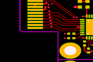
PCB geralmente consiste em quatro camadas, que são laminados termicamente em uma única camada. O material usado no PCB de cima para baixo inclui Silkscreen, Máscara de solda, Cobre e Substrato.
A última dessas camadas, substrato, é feito de fibra de vidro e também é conhecido como FR4, com as letras FR representando “retardador de fogo.” Esta camada de substrato fornece uma base sólida para PCBs, embora a espessura possa variar de acordo com os usos de uma determinada placa.
Também existe uma linha mais barata de placas no mercado que não utilizam os mesmos materiais de PCB mencionados acima., mas em vez disso consistem em fenólicos ou epóxis. Devido à sensibilidade térmica dessas placas, eles tendem a perder sua laminação facilmente. Essas placas mais baratas costumam ser fáceis de identificar pelo cheiro que exalam ao serem soldadas.
A segunda camada do PCB é cobre, que é laminado no substrato com uma mistura de calor e adesivo. A camada de cobre é fina, e em algumas placas existem duas dessas camadas – um acima e outro abaixo do substrato. PCBs com apenas uma camada de cobre tendem a ser usados para dispositivos eletrônicos mais baratos.
Acima da máscara de solda verde está a camada de serigrafia, que adiciona letras e indicadores numéricos que tornam um PCB legível para programadores de tecnologia. Esse, por sua vez, torna mais fácil para os montadores de eletrônicos colocar cada PCB no lugar adequado e na direção certa em cada componente. A camada da serigrafia geralmente é branca, embora cores como o vermelho, amarelo, cinza e preto também são usados às vezes.
Termos técnicos da camada PCB
Além de saber como o PCB é colocado em camadas, você deve saber que os termos técnicos acompanham o uso de PCBs:
• Anel anular. O anel de cobre que envolve os furos em uma PCB.
• RDC. Um acrônimo para verificação de regras de design. Essencialmente, RDC é uma prática pela qual o design de um PCB é verificado quanto à sua funcionalidade. Os detalhes verificados incluem a largura dos traços e furos.
• Golpe de perfuração. Usado para descrever todos os furos em uma PCB, se está correto ou errado. Em alguns casos, um furo pode estar ligeiramente incorreto devido ao equipamento de perfuração cego usado durante a produção.
• Dedo. Metal exposto ao longo da borda da placa que serve como pontos de conexão entre duas PCBs. Os dedos são encontrados com mais frequência em videogames antigos e cartões de memória.
• Bits de mouse. Uma seção de PCB excessivamente perfurada a ponto de ameaçar a integridade estrutural da placa.
• Almofada. Uma área de metal exposto em uma PCB, sobre a qual geralmente é aplicada uma peça soldada.
• Painel. Uma grande placa de circuito composta por placas menores, que eventualmente são separados para uso individual.
• Colar estêncil. Um estêncil de metal em uma placa, sobre o qual a pasta é colocada para soldar.
• Avião. Uma seção maior de cobre exposto em uma PCB, que é marcado por fronteiras, mas carece de caminho.
• Orifício passante banhado. Um buraco que passa direto por uma PCB, geralmente com a finalidade de conectar outro componente. O furo é banhado e geralmente apresenta um anel anular.
• Slot. Qualquer buraco que não seja circular. PCBs com slots costumam ter preços altos devido aos custos de produção para criar orifícios de formatos estranhos em uma placa de circuito. Os slots normalmente não são banhados.
• Montagem em superfície. Um método pelo qual as peças externas são montadas diretamente na placa de circuito impresso sem furos passantes.
• Rastreamento. Uma linha contínua de cobre através de um PCB.
• pontuação V. Um local onde a placa foi parcialmente cortada. Isso pode tornar um PCB vulnerável a quebras.
• Através de. Um buraco através do qual os sinais viajam entre camadas. Versões com tenda são cobertas com máscara de solda protetora, enquanto as vias não protegidas são usadas para conexões de conectores.
O número que precede uma camada refere-se ao número exato de camadas condutoras, seja uma camada de roteamento ou plana – os dois tipos de camada. As camadas tendem a ter o número 1, ou qualquer um dos próximos quatro números pares: 2, 4, 6, 8. As placas de camada às vezes têm números ímpares, mas estes são raros e dificilmente fariam qualquer diferença. Por exemplo, o material PCB em um 5 camada ou 6 placa de camada seria virtualmente idêntica.
Os dois tipos de camadas têm funções diferentes. Trilhas de recursos de camadas de roteamento. Camadas planas servem como conectores de energia e apresentam planos de cobre. As camadas planas também apresentam ilhas que determinam a finalidade de sinalização de uma placa., seja isso 3.3 V ou 5 V.