CO., LTD")
Distanțare minimă Producător PCB.A “Distanțare minimă Producător PCB” este specializată în realizarea de plăci de circuite imprimate cu o distanță incredibil de precisă și minimă între componentele electrice. Cu tehnologie de ultimă oră și atenție meticuloasă la detalii, produc plăci care maximizează eficiența și performanța în dispozitivele electronice compacte. Expertiza lor constă în depășirea limitelor designului pentru a crea PCB-uri care optimizează integritatea semnalului și minimizează interferențele. Fie pentru electronice de larg consum, aplicații aerospațiale, sau dispozitive medicale, plăcile lor stabilesc standardul pentru fiabilitate și miniaturizare în industrie.
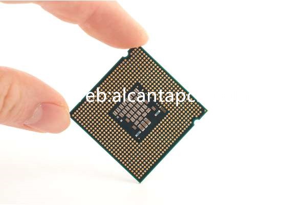
Ce este PCB cu spațierea minimă?
PCB cu pas minim se referă la distanța minimă admisă între diferitele căi conductoare, plăcuțe și componente în placa de circuit imprimat (PCB) proiecta. Aceste distanțe trebuie respectate cu strictețe în proiectare pentru a evita interferența semnalului, scurtcircuite și defecțiuni electrice. Pe măsură ce dispozitivele electronice devin din ce în ce mai miniaturizate și de înaltă performanță, cerințele pentru distanța minimă sunt, de asemenea, din ce în ce mai mari.
În design electronic modern, distanța minimă este un parametru crucial. Afectează direct performanța și fiabilitatea PCB-ului. Dacă distanța este prea mică, poate apărea diafonia semnalului între căile conductoare, provocând instabilitate sau chiar defecțiune a circuitului. Dacă distanța este prea mare, va risipi spațiu valoros la bord și va crește costurile de producție. Prin urmare, la proiectarea unui PCB, trebuie găsit un echilibru între performanță și cost.
Există mai mulți factori de luat în considerare atunci când proiectați un PCB cu pas minim. Prima este integritatea semnalului. Pe măsură ce frecvența de funcționare a echipamentelor electronice crește, creste si viteza de transmisie a semnalului. Acest lucru necesită o distanță suficientă între căile conductoare de pe PCB pentru a preveni interferența între semnalele de mare viteză. Al doilea este managementul termic. Proiectele de circuite de înaltă densitate sunt adesea însoțite de componente de mare putere care generează cantități mari de căldură atunci când funcționează. Designul de spațiere rezonabilă poate disipa eficient căldura și poate evita deteriorarea componentelor prin supraîncălzire.
În plus, limitările procesului de fabricație sunt un aspect important. Diferiți producători și procese au cerințe diferite de distanță minimă. În general vorbind, procesele convenționale de fabricare a PCB-ului pot atinge un pas minim de 6 mil (aproximativ 0,15 mm), în timp ce procesele avansate pot ajunge la 3mil (aproximativ 0,075 mm) sau chiar mai mici. La proiectarea PCB-urilor cu pas minim, designerii trebuie să lucreze îndeaproape cu producătorii pentru a se asigura că designul poate fi produs fără probleme.
Merită menționat că odată cu dezvoltarea tehnologiei, apar și unele materiale și tehnologii noi, oferind mai multe posibilități pentru proiectarea PCB cu pas minim. De exemplu, aplicarea unei plăci de circuite flexibile (FPC) și interconectare de înaltă densitate (HDI) tehnologia face posibilă realizarea unor pasuri mai mici. Plăcile de circuite flexibile au proprietăți bune de îndoire și pot fi utilizate în aplicații cu spațiu limitat. Tehnologia HDI realizează o densitate mai mare a cablurilor și o distanță mai mică prin microvia, găurire cu laser și tehnologie de laminare multistrat.
În general, designul PCB cu pas minim ocupă o poziție extrem de importantă în produsele electronice moderne. Nu numai că afectează în mod direct performanța și fiabilitatea circuitului, dar se referă și la costul produsului și la competitivitatea pieței. Odată cu progresul continuu al tehnologiei electronice, Designul PCB cu pas minim se va confrunta, de asemenea, cu mai multe provocări și oportunități. Designerii trebuie să învețe și să stăpânească în mod constant cele mai recente tehnologii și procese pentru a face față cerințelor în schimbare ale pieței. Prin optimizarea designului PCB cu pas minim, performanță mai mare, pot fi realizate produse electronice de dimensiuni mai mici și cu costuri mai mici, promovarea dezvoltării întregii industrii electronice.
Ghid de referință pentru proiectarea PCB a distanței minime.
Când proiectați un PCB cu pas minim, fiecare pas trebuie luat în considerare cu atenție pentru a asigura performanța și fiabilitatea circuitului. Mai jos sunt ghiduri detaliate de proiectare pentru a vă ajuta să implementați circuite de înaltă densitate, menținând în același timp calitatea și fabricabilitatea designului.
Planificarea designului
Planificarea designului este primul pas în proiectarea PCB cu pas minim. Primul, trebuie determinate cerințele generale și funcționalitatea circuitului, inclusiv performanța electrică, management termic, si rezistenta mecanica. În faza de planificare, acordați o atenție deosebită zonelor cu densitate mare, care conțin adesea un număr mare de componente și cablaje complexe. Prin identificarea acestor zone critice la începutul proiectării, componentele și rutarea pot fi aranjate mai eficient, asigurarea stabilității transmisiei semnalului și reducerea potențialelor probleme.
Proiectare schematică
Proiectarea schematică este procesul de conversie a structurii logice a unui circuit într-o diagramă vizuală. Utilizați software CAD, cum ar fi Eagle, Altium Designer sau KiCad pentru a desena scheme detaliate ale circuitelor. Asigurați-vă că toate componentele și conexiunile sunt reprezentate corect și conțin parametrii electrici necesari. În această etapă, concentrați-vă pe relația logică și secvența conexiunii dintre componente, care va afecta direct dispunerea PCB-ului și cablarea ulterioară.
Aspectul componentelor
Dispunerea componentelor este procesul de conversie a unei scheme de circuit într-un aspect fizic. Amplasați componentele în mod corespunzător pentru a asigura cea mai scurtă cale de semnal, reducând astfel latența și interferența semnalului. Dispunerea componentelor trebuie să ia în considerare performanța electrică și managementul termic pentru a evita ca componentele cu căldură ridicată să fie plasate una lângă alta pentru a preveni supraîncălzirea. Pentru circuite de înaltă frecvență, încercați să plasați componentele relevante cât mai aproape posibil pentru a reduce inductanța și capacitatea parazită și pentru a asigura integritatea semnalului.
Cablaj
Rutarea este o parte esențială a designului PCB cu pas minim. Urmați cerințele minime de distanță pentru rutare pentru a asigura integritatea semnalului și integritatea puterii. Aranjați în mod rezonabil locația liniilor de semnal și a liniilor de alimentare pentru a evita ca liniile de semnal să fie prea aproape de liniile de alimentare pentru a reduce interferențele electromagnetice. Pentru linii de semnal de mare viteză, încercați să utilizați căi scurte și drepte pentru a reduce reflexia și pierderea semnalului. Pentru PCB-uri multistrat, utilizați fiecare strat cu înțelepciune pentru a obține o distribuție optimă a semnalului și a puterii.
Verificați și verificați
După finalizarea plasării și direcționării, este esențial să se efectueze o verificare a regulilor de proiectare (RDC). Instrumentele DRC pot detecta automat erorile de proiectare și nerespectarea specificațiilor, asigurându-se că distanța îndeplinește cerințele minime. Verificați regulile electrice pentru a vă asigura că toate conexiunile sunt corecte și că nu există plăcuțe neconectate sau scurtcircuit. Verificați performanța electrică a designului pentru a vă asigura că transmisia semnalului și distribuția energiei îndeplinesc cerințele de proiectare.
Generați fișiere de producție
După ce proiectarea este finalizată și a trecut inspecția, sunt generate fișiere de fabricație care îndeplinesc cerințele minime de spațiere, inclusiv pile Gerber și pile de foraj. Fișierele Gerber conțin imagini ale fiecărui strat al PCB-ului, iar fișierele de foraj indică locația și dimensiunea găurilor care trebuie să fie forate. Aceste fișiere vor fi furnizate producătorului PCB ca bază pentru producție. Asigurați-vă că documentația este corectă și completă pentru a evita problemele în timpul producției.
Urmând instrucțiunile de mai sus, designerii pot proiecta eficient PCB-uri cu pas minim pentru a asigura performanță ridicată și fiabilitate ridicată a circuitului. Planificarea corectă și inspecția atentă pot reduce semnificativ erorile de proiectare și pot îmbunătăți calitatea și fabricabilitatea produsului.
Ce material este folosit în PCB cu spațierea minimă?
Alegerea materialelor potrivite joacă un rol vital în performanța PCB-urilor cu pas minim. Următoarele sunt câteva materiale utilizate în mod obișnuit și caracteristicile acestora:
FR4 (rășină epoxidică armată din fibră de sticlă)
FR4 este unul dintre cele mai comune materiale de substrat PCB și este adoptat pe scară largă datorită proprietăților sale electrice bune, rezistență mecanică și rentabilitate. Are o constantă dielectrică ridicată și rezistență la căldură, făcându-l potrivit pentru majoritatea aplicațiilor electronice. În modelele PCB cu pas minim, FR4 poate oferi conductivitate electrică stabilă și suport mecanic, contribuind la asigurarea fiabilității și stabilității transmisiei semnalului.
Placa de aluminiu
Aluminiu substraturi sunt adesea folosite în circuite care necesită performanțe ridicate de disipare a căldurii, precum iluminatul cu LED-uri și amplificatoarele de putere. Substratul din aluminiu are performanțe excelente de disipare a căldurii și conductivitate termică, care poate conduce eficient căldura de la dispozitivele de circuit către mediul extern, reducând astfel temperatura circuitului și îmbunătățind stabilitatea și fiabilitatea sistemului. În proiectarea PCB cu pas minim, aplicarea substratului de aluminiu poate rezolva eficient problemele de acumulare de căldură și evadarea termică și poate asigura funcționarea stabilă a circuitului.
Poliimidă
Poliimida este un material utilizat în mod obișnuit pentru plăcile de circuite flexibile, cu o flexibilitate excelentă și rezistență la temperaturi ridicate. Se poate îndoi în spații întortocheate și se poate adapta nevoilor de design ale formelor complexe, deci este deosebit de util în unele aplicații speciale. În modelele PCB cu pas minim, poliimida poate oferi soluții de proiectare flexibile, menținând în același timp performanțe electrice și fiabilitate bune.
Strat conductiv
Indiferent de materialul suport ales, alegerea stratului conductor este critică. De obicei, stratul conductor folosește folie de cupru, iar grosimea sa este în general de 1 oz/ft² (35μm). Folia de cupru are o conductivitate electrică bună și rezistență mecanică, și poate rezista la curentul și tensiunea de conectare din circuit. În design PCB cu pas minim, Grosimea corespunzătoare a stratului conductor poate asigura o bună transmisie a semnalului și performanță de conectare, oferind în același timp un suport mecanic suficient.
În concluzie, alegerea materialului potrivit este crucială pentru proiectarea PCB cu pas minim. Materialele diferite au caracteristici și domenii de aplicare diferite, și trebuie să fie selectate în mod rezonabil în funcție de nevoile reale în timpul procesului de proiectare pentru a asigura stabilitatea, fiabilitatea și optimizarea performanței circuitului.
Ce dimensiune are PCB cu spațierea minimă?
Alegerea materialelor potrivite joacă un rol vital în performanța PCB-urilor cu pas minim. Următoarele sunt câteva materiale utilizate în mod obișnuit și caracteristicile acestora:
FR4 (rășină epoxidică armată din fibră de sticlă)
FR4 este unul dintre cele mai comune materiale de substrat PCB și este adoptat pe scară largă datorită proprietăților sale electrice bune, rezistență mecanică și rentabilitate. Are o constantă dielectrică ridicată și rezistență la căldură, făcându-l potrivit pentru majoritatea aplicațiilor electronice. În modelele PCB cu pas minim, FR4 poate oferi conductivitate electrică stabilă și suport mecanic, contribuind la asigurarea fiabilității și stabilității transmisiei semnalului.
Placa de aluminiu
Substraturile din aluminiu sunt adesea folosite în circuite care necesită performanțe ridicate de disipare a căldurii, precum iluminatul cu LED-uri și amplificatoarele de putere. Substratul din aluminiu are performanțe excelente de disipare a căldurii și conductivitate termică, care poate conduce eficient căldura de la dispozitivele de circuit către mediul extern, reducând astfel temperatura circuitului și îmbunătățind stabilitatea și fiabilitatea sistemului. În proiectarea PCB cu pas minim, aplicarea substratului de aluminiu poate rezolva eficient problemele de acumulare de căldură și evadarea termică și poate asigura funcționarea stabilă a circuitului.
Poliimidă
Poliimida este un material utilizat în mod obișnuit pentru plăcile de circuite flexibile, cu o flexibilitate excelentă și rezistență la temperaturi ridicate. Se poate îndoi în spații întortocheate și se poate adapta nevoilor de design ale formelor complexe, deci este deosebit de util în unele aplicații speciale. În modelele PCB cu pas minim, poliimida poate oferi soluții de proiectare flexibile, menținând în același timp performanțe electrice și fiabilitate bune.
Strat conductiv
Indiferent de materialul suport ales, alegerea stratului conductor este critică. De obicei, stratul conductor folosește folie de cupru, iar grosimea sa este în general de 1 oz/ft² (35μm). Folia de cupru are o conductivitate electrică bună și rezistență mecanică, și poate rezista la curentul și tensiunea de conectare din circuit. În design PCB cu pas minim, Grosimea corespunzătoare a stratului conductor poate asigura o bună transmisie a semnalului și performanță de conectare, oferind în același timp un suport mecanic suficient.
În concluzie, alegerea materialului potrivit este crucială pentru proiectarea PCB cu pas minim. Materialele diferite au caracteristici și domenii de aplicare diferite, și trebuie să fie selectate în mod rezonabil în funcție de nevoile reale în timpul procesului de proiectare pentru a asigura stabilitatea, fiabilitatea și optimizarea performanței circuitului.
Procesul producătorului de PCB cu distanță minimă.
Fabricarea PCB-urilor cu pas minim implică o serie de etape precise ale procesului, fiecare pas este esențial pentru a se asigura că produsul final îndeplinește cerințele de proiectare și este de înaltă calitate.
Prima este etapa de pregătire a designului. În această etapă, inginerii trebuie să utilizeze software de proiectare asistată de computer pentru a genera fișiere standard Gerber și fișiere de foraj conform cerințelor minime de spațiere. Aceste fișiere conțin informații despre modelul și locația orificiilor de pe placa de circuit, oferind baza pentru fabricarea ulterioară.
Urmează fabricarea substratului. În acest pas, producătorii plasează folie de cupru pe materialul substratului. Materialul substratului este de obicei FR4, care are proprietăți bune de izolare și rezistență mecanică și este potrivit pentru majoritatea aplicațiilor. Prin acțiunea temperaturii și presiunii ridicate, folia de cupru și substratul sunt strâns combinate pentru a forma structura de bază a plăcii de circuite.
Aceasta este urmată de etapa de transfer a imaginii. În acest proces, producătorii folosesc adeziv fotosensibil sau fotorezist pentru a transfera modelul de circuit proiectat pe suprafața foliei de cupru prin tehnici de expunere și dezvoltare. Expunerea face ca stratul adeziv să se solidifice pentru a forma un șablon pentru modelul circuitului, în timp ce dezvoltarea îndepărtează părțile neexpuse, lăsând modelul de circuit dorit.
Apoi urmează pasul de gravare. În această etapă, producătorul plasează placa de circuit într-o soluție de gravare, care îndepărtează porțiunile neprotejate ale foliei de cupru, lăsând în urmă un model de circuit care îndeplinește cerințele minime de distanță. Procesul de gravare utilizează de obicei coroziune chimică sau coroziune electrochimică pentru a se asigura că modelul este clar și precis.
Urmează etapa de forare. În acest pas, producătorii folosesc mașini de găurit de înaltă precizie pentru a găuri prin și găuri oarbe pentru conexiunile electrice și montarea componentelor. Aceste găuri trebuie să fie poziționate cu precizie pentru a asigura integritatea funcțională și fiabilitatea plăcii de circuite.
Aceasta este urmată de galvanizare și tratarea suprafeței. În timpul acestui proces, producătorii plăci de circuite electroplate pentru a spori conductivitatea și durabilitatea. În plus, masca de lipit și straturi de ecran de mătase sunt aplicate pe suprafața plăcii de circuit pentru a proteja circuitul și pentru a facilita identificarea.
În sfârșit vine faza de testare și inspecție. În timpul acestui pas, producătorul efectuează teste electrice și inspecții optice ale plăcii de circuit pentru a se asigura că îndeplinește cerințele minime de distanță și că nu prezintă defecte. Numai după ce au trecut teste și inspecții stricte, placa de circuit poate fi considerată un produs calificat și livrată clienților pentru utilizare.
În concluzie, fabricarea PCB cu pas minim este un proces complex și precis care necesită un control strict al calității și tehnici de operare sofisticate. Urmând procese de fabricație standardizate, se poate asigura că produsul final are performanță și fiabilitate excelente pentru a răspunde nevoilor diferitelor dispozitive electronice.
Zona de aplicare a PCB cu spațierea minimă.
PCB cu pas minim este utilizat pe scară largă în diverse domenii, iar designul său de înaltă densitate și de înaltă performanță îl fac prima alegere pentru multe dispozitive electronice. Următoarele sunt aplicațiile PCB cu pas minim în diferite domenii:
Electronica de consum
Electronice de larg consum, cum ar fi smartphone-urile, tablete, iar ceasurile inteligente reprezintă provocări pentru designul PCB. Pe măsură ce aceste dispozitive devin din ce în ce mai miniaturizate și bogate în funcții, PCB-urile trebuie să îndeplinească cerințe de performanță mai ridicate și design mai compact. Designul PCB cu pas minim joacă un rol vital în aceste dispozitive, asigurând stabilitatea și fiabilitatea circuitului.
Calculatoare și echipamente de rețea
În calculatoare și echipamente de rețea, precum plăcile de bază, plăci grafice, și routere, PCB-urile cu pas minim joacă, de asemenea, un rol cheie. Aceste dispozitive trebuie să proceseze cantități mari de date și semnale, necesitând astfel proiecte de circuite de mare viteză și densitate mare. Aplicarea PCB cu pas minim asigură performanța și fiabilitatea acestor dispozitive.
Electronica vehiculului
Domeniul electronicii auto impune cerințe unice pentru proiectarea PCB-urilor. De la computere de bord la module de senzori, electronicele auto trebuie să poată funcționa stabil în condiții de mediu dure. Designul PCB cu pas minim poate îmbunătăți capacitatea anti-interferență și fiabilitatea circuitului și poate asigura funcționarea normală a echipamentelor electronice auto.
Control industrial
Domeniul controlului industrial necesită sisteme de control stabile și fiabile pentru a asigura desfășurarea fără probleme a procesului de producție. Echipamente precum PLC-uri (Controlere logice programabile) iar convertizoarele de frecvență folosesc adesea modele de PCB cu pas minim pentru a îndeplini cerințele ridicate din mediile industriale. Aceste dispozitive necesită design de circuite cu capacități anti-interferențe ridicate și stabilitate pentru a asigura funcționarea normală a producției industriale.
Echipament medical
În domeniul echipamentelor medicale, precum electrocardiografie și echipamente de monitorizare medicală, cerințe stricte sunt impuse pentru proiectarea PCB. Aceste dispozitive necesită un design de circuit stabil și fiabil pentru a asigura colectarea și transmiterea exactă a datelor medicale. Aplicarea PCB cu pas minim poate îmbunătăți performanța și fiabilitatea echipamentului medical și poate asigura siguranța și sănătatea pacienților.
În concluzie, PCB cu pas minim are valoare de aplicare importantă în domeniul electronicelor de larg consum, echipamente informatice și de rețea, electronice auto, control industrial si echipamente medicale. Designul său de înaltă performanță și fiabilitate oferă o garanție fiabilă pentru funcționarea normală a diferitelor dispozitive electronice și promovează dezvoltarea și progresul științei și tehnologiei moderne.
Care sunt avantajele Minimum Spacing PCB?
Avantajele PCB cu pas minim sunt evidente, și au un impact pozitiv asupra performanței și fiabilității echipamentelor electronice. Iată o privire mai atentă asupra beneficiilor PCB-urilor cu pas minim:
Fiabilitate ridicată
Cerințele minime de proiectare pentru PCB sunt stricte, care poate reduce eficient riscul defecțiunilor electrice și scurtcircuitelor. Prin setări rezonabile de spațiere, interferența semnalului și încrucișarea pot fi evitate, îmbunătățind astfel stabilitatea și fiabilitatea circuitului. Această fiabilitate ridicată este crucială pentru aplicații critice, cum ar fi echipamentele medicale și aerospațiale, asigurarea functionarii stabile a echipamentului pe o perioada indelungata de timp.
Miniaturizare
Proiectarea PCB-ului cu pas minim permite un aspect mai compact al circuitului, permițând astfel miniaturizarea și ușurarea dispozitivelor electronice. Pe măsură ce cerințele privind dimensiunea și greutatea electronicelor de larg consum continuă să crească, miniaturizarea a devenit o tendință importantă în design. Prin PCB cu pas minim, mai multe funcții pot fi implementate într-un spațiu limitat, îmbunătățirea competitivității produselor și a experienței utilizatorului.
Performanță ridicată
Designul PCB cu pas minim ajută la îmbunătățirea ratei de transmisie a semnalului și a integrității. Setările rezonabile de cablare și distanță pot reduce întârzierea și distorsiunea transmisiei semnalului, îmbunătățind astfel performanța circuitului și viteza de răspuns. Pentru transmiterea de semnale digitale de mare viteză și semnale analogice, designul PCB cu pas minim este deosebit de important pentru a asigura transmisia și procesarea exactă a semnalelor.
Eficiența producției
PCB cu pas minim adoptă un proces de producție standardizat, care poate îmbunătăți eficiența producției și poate reduce costurile. În timpul procesului de fabricație, respectarea strictă a specificațiilor de proiectare și a cerințelor de spațiere poate reduce reparațiile și reparațiile inutile, economisind timp și costuri cu forța de muncă. În același timp, procesele de producție standardizate pot reduce, de asemenea, risipa de materiale și erorile de fabricație, și să îmbunătățească consistența și fiabilitatea produsului.
Usor de intretinut
Designul PCB cu pas minim îndeplinește specificațiile stricte de proiectare și facilitează diagnosticarea și repararea dispozitivului. Setările rezonabile de dispunere și spațiere pot face piesele defecte mai ușor de localizat și înlocuit, scurtează timpul de întreținere, și reduce costurile de întreținere. Acest lucru este de mare importanță pentru echipamentele care necesită întreținere și întreținere frecventă, precum sistemele industriale de control și echipamentele de comunicații, pentru a minimiza timpul de nefuncţionare şi pierderile de producţie.
În concluzie, PCB cu pas minim nu poate îmbunătăți doar performanța și fiabilitatea echipamentelor electronice, dar și reducerea costurilor de producție și întreținere. Este unul dintre factorii cheie indispensabili în designul electronic modern.
FAQ
Care este standardul pentru PCB cu pas minim?
Standardele PCB cu pas minim variază în funcție de diferite aplicații și procese de fabricație. În general vorbind, fiecare țară și regiune are propriile standarde de proiectare PCB, inclusiv reglementări privind distanța minimă, lățimea minimă a liniei, deschidere minima, etc.. De obicei, inginerul proiectant va proiecta conform regulilor de proiectare furnizate de producătorul selectat sau de fabrica de producție de PCB pentru a se asigura că proiectul final de PCB îndeplinește cerințele de fabricație.
Cum să alegeți materialul PCB cu pas minim?
La selectarea materialelor PCB cu pas minim, Trebuie să fie luați în considerare mai mulți factori, inclusiv performanța electrică, performanta termica, rezistență mecanică și cost. Materialele PCB comune includ FR4, substrat de aluminiu, Polimed, etc.. Pentru circuite de înaltă frecvență și de mare viteză, precum frecvența radio (RF) circuite sau circuite digitale de mare viteză, poate fi necesar să se selecteze materiale speciale cu constante dielectrice și pierderi dielectrice mai mici. În plus, disponibilitatea materialului și costul trebuie luate în considerare pentru a asigura conformitatea cu bugetul și calendarul proiectului.
Cât durează fabricarea PCB cu pas minim?
Timpul minim de fabricație pentru PCB depinde de mai mulți factori, inclusiv complexitatea PCB, Numărul de straturi, cantitate, și capacitățile de producție și volumul de muncă ale producătorului selectat sau ale fabricii de producție de PCB. În general vorbind, timpul ciclului de fabricație pentru un PCB simplu cu două fețe poate fi între câteva zile și o săptămână, în timp ce un PCB complex cu mai multe straturi poate dura mai mult, posibil câteva săptămâni pentru a finaliza producția și testarea.
Cum se efectuează verificări ale designului PCB cu pas minim?
Când se efectuează verificări de proiectare a PCB cu pas minim, Verificarea regulilor de proiectare (RDC) instrumentele sunt adesea folosite. Aceste instrumente pot verifica automat dacă distanța, lățimea liniei, deschiderea și alți parametri din proiectare respectă regulile predefinite. De asemenea, inginerii proiectanți pot revizui manual proiectul și pot efectua inspecții vizuale și electrice pentru a se asigura că PCB îndeplinește cerințele minime de spațiu. În plus, efectuarea de revizuiri multiple de proiectare în timpul etapei de proiectare este, de asemenea, unul dintre pașii importanți pentru a asigura calitatea PCB.