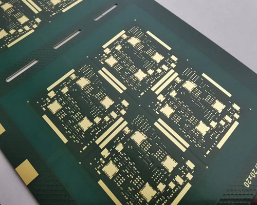
에 대한 연락하다 |
전화: +86 (0)755-8524-1496
이메일: info@alcantapcb.com
다층 PCB

다층 PCB

PCB 제조, We offer Multilayer PCB from 4 레이어 108 layer. HDI PCBs. Rigid-Flex HDI PCB. 하이브리드 & 혼합 유전체, Buried and Blind Vias Technologies.


The Buried Holes and Blind Holes are Defined as Follows

Blind Vias: A blind via is a type of via that connects the inner trace of the PCB to the trace of the PCB surface. This hole does not penetrate the entire board.
Buried Vias: Buried vias are only connected to the type of vias between the inner layers, so they are not visible from the surface of the PCB.

Advantages of Blind Buried Hole Printed Circuit Board

  • Eliminate a large number of through-hole designs and increase wiring density and package density;
  • Diversify and complicate the design of the interconnect structure of the multi-layer board;
  • Significantly improved the reliability of multi-layer boards and the electrical performance of electronic products.

The Following Three Points are Distinguished for Blind Buried Plate Boards

  • In contrast to the through hole, the through hole refers to a hole through which each layer is drilled, and the blind hole is a non-drilled through hole.
  • Blind hole subdivision: blind hole, buried hole (outer layer is not visible).
  • Distinguish from the production process: blind holes are drilled before pressing, and through holes are drilled after pressing.

Blind buried hole technology is mainly used on relatively high-end PCBs, with high technical content and high requirements for PCB board manufacturers. 우리의 이메일: info@alcantapcb.com


이전:

다음: