CO., LTD")
Producător de PCB-uri RF. Un producător de PCB-uri RF este specializat în proiectarea și producerea de plăci de circuite imprimate pentru aplicații cu frecvență radio.. Aceste PCB -uri sunt esențiale pentru transmiterea semnalelor de înaltă frecvență în dispozitivele de comunicație fără fir, Sisteme radar, și tehnologie prin satelit. Producătorul asigură calitate înaltă, fabricație precisă pentru a îndeplini cerințele stricte de performanță RF, inclusiv integritatea semnalului și interferența minimă, oferind soluții fiabile pentru electronice avansate.
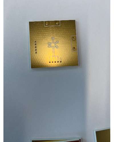
PCB-uri RF (Plăci de circuite imprimate cu frecvență radio) sunt plăci de circuite specializate concepute pentru a funcționa la frecvențe radio, de obicei variind de la 3 kHz la 300 GHz. Aceste PCB-uri sunt critice în aplicațiile care necesită o transmisie precisă și eficientă a semnalului, cu pierderi și distorsiuni minime. Acest articol explorează proprietățile, structura, materiale, procesele de fabricatie, aplicații, avantaje, și întrebări frecvente (Întrebări frecvente) legate de PCB-urile RF.
Structura PCB-urilor RF
Structura PCB-urilor RF este proiectată meticulos pentru a susține de înaltă frecvență integritatea și performanța semnalului:
Substratul este de obicei realizat din materiale cu o constantă dielectrică scăzută și tangentă de pierdere, cum ar fi ptfe (politetrafluoroetilenă), laminate Rogers, sau compozite PTFE umplute cu ceramică. Aceste materiale ajută la minimizarea pierderilor de semnal și asigură o performanță stabilă la frecvențe înalte.
Pentru urme se folosesc straturi subțiri de cupru sau alte metale conductoare, asigurând pierderi minime de semnal și performanță de înaltă frecvență. Aceste straturi sunt adesea gravate cu precizie pentru a forma modelele de circuit necesare.
Materialele dielectrice de înaltă performanță sunt folosite pentru a separa straturile conductoare, menținerea izolației electrice și a integrității semnalului. Aceste straturi sunt cruciale pentru prevenirea interferențelor semnalului și a diafoniei între urmele adiacente.
Planurile de masă dedicate oferă un plan de referință pentru semnale, reducerea interferențelor electromagnetice (EMI) și îmbunătățirea calității semnalului. Planurile de sol joacă, de asemenea, un rol vital în managementul termic prin disiparea căldurii generate de operațiunile de înaltă frecvență.
Interconexiunile verticale conectează diferite straturi ale PCB-ului, permițând rutare complexă și design de înaltă densitate. Microvias, în special, sunt utilizate în interconectarea de înaltă densitate (HDI) proiecte pentru a minimiza inductanța și capacitatea parazitară.
Acoperiri de protecție precum ENIG (Electroless Nichel Immersion Gold) sau OSP (Conservanți organici de lipit) sunt folosite pentru a îmbunătăți lipirea și pentru a proteja împotriva oxidării. Aceste finisaje contribuie, de asemenea, la asigurarea unor conexiuni electrice fiabile.
Materiale utilizate în PCB-uri RF
Materialele cheie utilizate în PCB-urile RF includ:
Un material dielectric cu pierderi reduse, cunoscut pentru performanța și stabilitatea excelentă la frecvență înaltă. PTFE este adesea folosit în aplicații care necesită o atenuare minimă a semnalului și o integritate ridicată a semnalului.
Laminate de înaltă performanță cu constantă dielectrică scăzută și tangentă de pierdere, conceput special pentru aplicații RF și microunde. Materialele Rogers sunt preferate pentru proprietățile lor electrice consistente și fiabilitatea la frecvențe înalte.
Aceste materiale oferă un echilibru de pierderi reduse, conductivitate termică ridicată, și stabilitate mecanică. Ele sunt adesea folosite în aplicații în care managementul termic și robustețea mecanică sunt critice.
Cuprul de înaltă puritate este utilizat pentru urme conductoare datorită conductibilității și fiabilității sale electrice excelente. Rezistența scăzută a cuprului ajută la menținerea integrității semnalului la frecvențe înalte.
Materiale cu constantă dielectrică scăzută și tangentă de pierderi, precum teflonul (Ptfe) și materiale Rogers specializate, sunt utilizate pentru a asigura pierderea și distorsiunea minimă a semnalului. Aceste materiale sunt cruciale pentru menținerea calității ridicate a semnalului.
Procesul de fabricație al PCB-urilor RF
Procesul de fabricație pentru PCB-uri RF implică mai mulți pași precisi pentru a asigura performanța și fiabilitatea de înaltă frecvență:
Alegerea materialelor de bază și a straturilor conductoare adecvate pe baza cerințelor de performanță. Procesul de selecție ia în considerare factori precum constanta dielectrică, tangenta de pierderi, proprietăți termice, si rezistenta mecanica.
Stivuirea și legarea mai multor straturi de materiale conductoare și dielectrice în condiții controlate pentru a forma un PCB stabil. Acest proces asigură grosimea și alinierea consistentă a stratului.
Găurire de precizie pentru a crea căi și microvii pentru interconexiuni verticale între straturi. Tehnicile avansate de foraj cu laser sunt adesea folosite pentru microvias pentru a obține o precizie ridicată și o deteriorare minimă a materialelor din jur.
Galvanizarea cuprului pe substrat și a canalelor interioare pentru a stabili conexiuni electrice fiabile. Acest pas asigură căi puternice și conductoare pentru transmisia semnalului.
Utilizarea fotolitografiei și a gravării chimice pentru a defini modelele de circuite și interconexiunile. Modelarea precisă este esențială pentru a obține aspectul și performanța dorite a circuitului.
Aplicarea straturilor de protecție pe suprafețele expuse de cupru pentru a îmbunătăți lipirea și a proteja împotriva oxidării. Finisajele suprafețelor ajută, de asemenea, la prevenirea coroziunii și asigură fiabilitatea pe termen lung.
Atașarea componentelor folosind tehnici de lipire potrivite pentru aplicații de înaltă frecvență, asigurând pierderi și distorsiuni minime ale semnalului. Procesul de asamblare include plasarea și lipirea atentă a componentelor RF pentru a menține integritatea semnalului.
Testare riguroasă pentru performanța electrică, integritatea semnalului, și respectarea specificațiilor de proiectare. Testarea include măsurători ale pierderii semnalului, verificări de impedanță, și cicluri termice pentru a asigura fiabilitatea în condiții de funcționare.
Aplicații ale PCB-urilor RF
PCB-urile RF sunt utilizate într-o gamă largă de aplicații de înaltă frecvență, inclusiv:
Stații de bază, antene, și module RF pentru rețelele de comunicații mobile și fără fir. PCB-urile RF sunt esențiale pentru transmiterea și recepția semnalelor de înaltă frecvență în sistemele de comunicații.
Sisteme radar de înaltă frecvență utilizate în apărare, aerospațial, și aplicații auto. PCB-urile RF permit procesarea și transmisia precisă a semnalului în sistemele radar.
Echipamente de diagnostic și imagistică, precum aparatele RMN și cu ultrasunete, care necesită procesare a semnalului de înaltă frecvență. PCB-urile RF asigură transmisie precisă și fiabilă a semnalului în dispozitivele medicale.
Transpondere, receptoare, și emițătoare utilizate în sistemele de comunicații prin satelit. PCB-urile RF acceptă legături de comunicație de înaltă frecvență în sistemele prin satelit.
Senzori de înaltă frecvență și sisteme de control utilizate în mediile de producție și control al proceselor. PCB-urile RF permit procesarea semnalului fiabilă și eficientă în automatizarea industrială.
Avantajele PCB-urilor RF
PCB-urile RF oferă câteva avantaje semnificative:
Proiectat pentru a suporta frecvențe RF cu pierderi și distorsiuni minime ale semnalului. PCB-urile RF asigură o integritate ridicată a semnalului și performanță la frecvențe înalte.
Menține calitatea și integritatea semnalului prin utilizarea de materiale cu pierderi reduse și procese de fabricație precise. PCB-urile RF reduc la minimum atenuarea semnalului și interferența.
Construcția robustă și testarea asigură performanța și fiabilitatea pe termen lung în aplicațiile solicitante de înaltă frecvență. PCB-urile RF sunt construite pentru a rezista la condiții dure de operare.
Disiparea eficientă a căldurii prin materialele substratului și caracteristicile de proiectare, asigurând o funcționare stabilă în condiții de mare putere. PCB-urile RF previn supraîncălzirea și deteriorarea termică.
Potrivit pentru o gamă largă de aplicații de înaltă frecvență din diverse industrii. PCB-urile RF pot fi personalizate pentru a îndeplini cerințele specifice de design și performanță.
FAQ
Ce materiale sunt utilizate de obicei pentru PCB-urile RF, si de ce?
PCB-urile RF folosesc de obicei materiale precum PTFE, laminate Rogers, și compozite PTFE umplute cu ceramică pentru constanta lor dielectrică scăzută, tangentă cu pierderi reduse, și stabilitate de înaltă frecvență. Aceste materiale sunt esențiale pentru menținerea integrității și performanței semnalului.
Cum diferă PCB-urile RF de PCB-urile standard?
PCB-urile RF sunt proiectate special pentru aplicații de înaltă frecvență, folosind materiale specializate și procese de fabricație pentru a minimiza pierderea și distorsiunea semnalului. PCB-urile standard sunt utilizate în mod obișnuit pentru aplicații cu frecvență mai mică și este posibil să nu necesite caracteristici de performanță atât de stricte.
Ce industrii beneficiază cel mai mult de pe urma utilizării PCB-urilor RF?
Industrii precum telecomunicațiile, aerospațial și de apărare, dispozitive medicale, comunicații prin satelit, și automatizarea industrială beneficiază semnificativ de utilizarea PCB-urilor RF datorită performanței și fiabilității lor de înaltă frecvență.
Cum sunt testate PCB-urile RF pentru a asigura fiabilitatea?
PCB-urile RF sunt supuse unor procese de testare riguroase, inclusiv testarea electrică pentru integritatea și performanța semnalului, Ciclism termic, și testarea fiabilității. Aceste teste asigură că PCB-urile RF îndeplinesc standardele stricte de performanță și durabilitate de înaltă frecvență.