CO., LTD")
Producător de substraturi pentru ambalaje FC-BGA ultra-multistrat. Suntem specializați în realizarea de substraturi pentru pachete FC-BGA cu mai multe straturi, folosind tehnologie de ultimă oră pentru a satisface cerințele interconexiunilor de înaltă densitate în dispozitivele electronice. Expertiza noastră constă în proiectarea și fabricarea substraturilor care oferă performanțe superioare, fiabilitate, si eficienta, satisfacerea nevoilor în evoluție ale industriei electronice.
Odată cu dezvoltarea continuă a echipamentelor electronice, cererea de înaltă performanță, plăcile de circuite de înaltă densitate continuă să crească. Ca tehnologie avansată, ultra-multistrat FC-BGA substratul de ambalare devine treptat o alegere ideală pentru a satisface această cerere. Acest articol va aprofunda caracteristicile, aplicații și avantaje ale FC-BGA ultra-multistrat substraturi de ambalare.
Ce sunt substraturile pentru pachete Ultra-Multistrat FC-BGA?
Ultra-Multilayer FC-BGA Package Substrates este o tehnologie de placă de circuit imprimată foarte integrată care utilizează tehnologia ultra-multistrat și ambalaj FC-BGA. În această tehnologie, plăcile de circuite multistrat sunt combinate prin procese de stivuire și interconectare de precizie, în timp ce utilizați Fine-Pitch Ball Grid Array (FC-BGA) ambalaj pentru a realiza proiecte de circuite de înaltă performanță și de înaltă densitate.
Principalele caracteristici ale acestei tehnologii includ:
Design de înaltă densitate: Prin tehnologia de stivuire multistrat, se realizează o densitate mai mare a circuitului și integrarea componentelor, care este potrivit pentru proiectarea circuitelor complexe și poate îndeplini cerințele de înaltă performanță și densitate ridicată ale echipamentelor electronice moderne.
Ambalaj FC-BGA: Folosind ambalaj FC-BGA, placa de circuit are o integrare mai mare și o dimensiune mai mică a pachetului, menținând în același timp performanțe ridicate, făcându-l potrivit pentru scenarii de aplicare cu spațiu limitat.
Design optimizat: Prin optimizarea aspectului și a designului de ecranare, interferența electromagnetică dintre plăcile de circuit este redusă, stabilitatea transmisiei semnalului este îmbunătățită, iar fiabilitatea și stabilitatea plăcii de circuite sunt asigurate.
Gamă largă de aplicații: Substraturile pentru pachete FC-BGA ultra-multistrat sunt utilizate pe scară largă în echipamentele de comunicații, electronice auto, Echipament medical, automatizări industriale și alte domenii, oferind soluții de înaltă performanță și fiabilitate pentru diverse aplicații.
În scurt, introducerea tehnologiei Ultra-Multilayer FC-BGA Package Substrates oferă noi posibilități pentru dezvoltarea echipamentelor electronice și oferă soluții mai eficiente și mai fiabile pentru scenarii de aplicare în diverse industrii.
Ghid de referință pentru proiectarea suporturilor pentru pachete Ultra-Multistrat FC-BGA.
Substratul de ambalare ultra-multistrat FC-BGA este o tehnologie avansată de circuite imprimate care oferă suport important pentru proiectarea dispozitivelor electronice de înaltă performanță. Următoarele sunt principalele conținuturi ale ghidului de referință de proiectare:
Substratul de ambalare ultra-multistrat FC-BGA folosește tehnologia de stivuire cu mai multe straturi pentru a realiza funcții de circuit foarte integrate printr-un aspect precis și un design de interconectare. Procesul de proiectare ar trebui să ia în considerare pe deplin factori precum aspectul circuitului, integritatea semnalului, și managementul termic.
Dispunerea corectă este cheia pentru a asigura performanța și fiabilitatea plăcii de circuite. În timpul procesului de layout, locațiile componentelor și căile semnalului ar trebui optimizate pe baza funcțiilor circuitului și a cerințelor de transmisie a semnalului pentru a minimiza interferența semnalului și diafonia.
Designul substratului de ambalare Ultra-Multilayer FC-BGA ar trebui să ia în considerare integritatea semnalului, inclusiv viteza de transmisie a semnalului, lungimea liniei de transmisie, potrivirea impedanței și alți factori. Tehnologii precum transmisia diferențială a semnalului și structura ierarhică între straturile de semnal sunt utilizate pentru a îmbunătăți stabilitatea și fiabilitatea transmisiei semnalului..
Datorită creșterii integrării ridicate și a densității de putere, managementul termic a devenit o problemă importantă în proiectarea substratului pachetului Ultra-Multilayer FC-BGA. Trebuie utilizate un design și materiale adecvate de disipare a căldurii pentru a se asigura că placa de circuite menține o performanță bună de disipare a căldurii atunci când funcționează la sarcini mari..
Selectarea pachetului FC-BGA adecvat este una dintre deciziile cheie în procesul de proiectare. Tipul și densitatea pachetului adecvate trebuie selectate pe baza unor factori precum complexitatea circuitului, cerințele de putere, și constrângeri de spațiu pentru a obține performanță și fiabilitate optime.
Procesul de fabricație al substratului de ambalare Ultra-Multistrat FC-BGA necesită control de înaltă precizie a procesului și echipamente avansate de producție. Proiectanții ar trebui să lucreze îndeaproape cu producătorii pentru a se asigura că proiectul îndeplinește cerințele de fabricație și pentru a efectua verificarea necesară a proiectului și testarea eșantioanelor..
Ghidul de referință pentru proiectarea substratului pachetului Ultra-Multilayer FC-BGA este conceput pentru a ajuta designerii să înțeleagă pe deplin caracteristicile și punctele de design ale acestei tehnologii, pentru a o aplica mai bine la proiectarea echipamentelor electronice performante. Prin aspect rezonabil, integritatea semnalului și proiectarea managementului termic, performanța ridicată și fiabilitatea plăcii de circuite pot fi atinse și promovează dezvoltarea continuă a tehnologiei electronice.
Ce dimensiune au substraturile de pachete Ultra-Multilayer FC-BGA?
Substratul de ambalare ultra-multistrat FC-BGA utilizează o serie de materiale de înaltă performanță pentru a-și asigura performanța excelentă la densitate mare., aplicații de mare viteză și de înaltă fiabilitate. Materialele principale includ:
Material de substrat: Materialul de bază al substratului de ambalare ultra-multistrat FC-BGA este, de obicei, rășina epoxidice armată cu fibră de sticlă de înaltă performanță. (FR-4) sau poliimidă (Pi). Aceste materiale au o excelentă rezistență mecanică și stabilitate termică. și performanța izolației electrice, capabil să îndeplinească cerințele de proiectare a circuitelor complexe.
Material strat conductiv: Stratul conductiv al substratului pachetului ultra-multistrat FC-BGA utilizează de obicei folie de cupru de înaltă puritate pentru a asigura performanțe conductoare bune și conexiuni de lipire fiabile. Folia de cupru are o bună conductivitate electrică și procesabilitate, și poate satisface nevoile de transmisie a semnalului de mare viteză și aspect de înaltă densitate.
Material strat izolator: În substratul de ambalare super multi-strat FC-BGA, stratul izolator joaca rolul de izolare si suport. Pânză din fibră de sticlă sau pânză subțire din fibră de sticlă impregnată cu rășină epoxidică (Prepreg) este de obicei folosit. Aceste materiale au proprietăți bune de izolare. si rezistenta mecanica, care poate izola eficient circuitul dintre straturile conductoare și poate oferi un suport stabil.
Material de lipit: Materialul de lipit al substratului pachetului ultra-multistrat FC-BGA utilizează de obicei lipire fără plumb sau lipire la temperatură joasă pentru a asigura fiabilitatea și protecția mediului a conexiunii de lipit.. Aceste materiale de lipit au performanțe bune de sudare și stabilitate termică, și poate îndeplini cerințele de sudare la temperatură înaltă și funcționare stabilă pe termen lung.
Material masca de lipit: Masca de lipit este folosită pentru a acoperi suprafața plăcii de circuit pentru a proteja firele și plăcuțele. De obicei, folosește un amestec de rășină epoxidice și pigmenți. Are o rezistență bună la căldură, rezistență chimică și rezistență la uzură, și poate preveni eficient lipirea. Scurtcircuit și oxidarea metalelor.
În concluzie, substratul de ambalare ultra-multistrat FC-BGA utilizează o serie de materiale de înaltă calitate, inclusiv materiale suport de înaltă performanță, materiale de strat conductiv, materiale de strat izolator, materiale de lipit și materiale de masca de lipit, asigurându-i densitatea mare , performanță și stabilitate excelente în aplicații de mare viteză și de înaltă fiabilitate.
Procesul de producție al substraturilor de pachete FC-BGA ultra-multistrat.
Procesul de fabricație al substratului de ambalare ultra-multistrat FC-BGA a trecut printr-o serie de etape de proces precise și complexe pentru a-i asigura performanța și fiabilitatea înalte.. Mai jos este o prezentare generală a principalelor sale procese de fabricație:
Pregătirea substratului: Primul pas în procesul de fabricație este pregătirea substratului. Alegeți materiale suport de înaltă calitate, cum ar fi epoxidul armat cu fibră de sticlă (FR-4) pentru a asigura rezistența mecanică și performanța electrică a plăcii de circuite. Substratul este curățat și tratat la suprafață pentru pregătirea etapelor ulterioare ale procesului.
Stivuire și laminare: TSubstratul de ambalare ultra-multistrat FC-BGA utilizează tehnologia de stivuire multistrat pentru a stivui mai multe plăci de circuite cu un singur strat în conformitate cu cerințele de proiectare. În timpul procesului de laminare, adeziv conductiv sau folie de cupru este acoperită între fiecare strat de plăci de circuite pentru a forma un strat de interconectare. Apoi, plăcile de circuite stivuite sunt presate împreună într-un singur corp printr-un proces de laminare pentru a forma o structură de plăci de circuite multistrat.
Prelucrare folie de cupru: Suprafața plăcii de circuite laminate multistrat este acoperită cu folie de cupru pentru a forma un strat conductor. Conform cerințelor de proiectare, metode precum gravarea chimică sau gravarea mecanică sunt utilizate pentru a îndepărta sau îndepărta excesul de folie de cupru pentru a forma modelul de circuit și orificiile de conectare ale plăcii de circuite..
Inspecția produsului finit: Inspecția strictă a calității este necesară în fiecare etapă a procesului de fabricație. După finalizarea procesării foliei de cupru, placa de circuit este inspectată pentru aspect, măsurare dimensională, și testarea conectivității la linie pentru a se asigura că calitatea fiecărei plăci de circuite îndeplinește cerințele standard.
Tratarea suprafeței: Aplicați un strat protector de cupru sau pastă de lipit pe suprafața plăcii de circuit pentru a îmbunătăți performanța de lipire și protecția împotriva coroziunii. Procesul de tratare a suprafeței include, de asemenea, metalizarea prin pulverizare pentru a forma un strat de metal lipit pe suprafața plăcii de circuite.
Testarea și ambalarea produsului finit: Substratul de ambalare FC-BGA ultra-multistrat fabricat trebuie să fie supus testării funcționale finale și testelor de fiabilitate pentru a se asigura că performanța și fiabilitatea sa îndeplinesc cerințele de proiectare. Prin testarea de îmbătrânire la temperatură înaltă, testarea performanței electrice și alte mijloace, se verifică stabilitatea plăcii de circuite în diverse medii de lucru. În cele din urmă, plăcile de circuite testate sunt ambalate pentru a preveni deteriorarea în timpul transportului și depozitării.
În general, procesul de fabricație a substraturilor de ambalare FC-BGA ultra-multistrat implică mai multe etape precise ale procesului și necesită un grad ridicat de suport tehnic și echipament. Prin control și testare stricte a calității, sunt asigurate performanța ridicată și fiabilitatea plăcilor de circuite, satisfacerea nevoilor de mare densitate, plăci de circuite de înaltă performanță în diverse scenarii de aplicare.
Zona de aplicare a substraturilor de pachete Ultra-Multilayer FC-BGA.
Substraturile de ambalare ultra-multistrat FC-BGA sunt utilizate pe scară largă în diverse domenii. În primul rând, joacă un rol cheie în domeniul comunicațiilor, utilizat pentru transmisia de date de mare viteză și echipamentele de comunicație în rețea, precum routerele, întrerupătoare, etc.. Densitatea sa ridicată și designul optimizat permit echipamentelor de comunicații să atingă viteze mai rapide de transmisie a semnalului și conexiuni de rețea mai stabile, îndeplinirea cerințelor stricte de performanță și fiabilitate ale sistemelor moderne de comunicații.
În al doilea rând, în domeniul electronicii auto, Substraturile de ambalare ultra-multistrat FC-BGA sunt utilizate pe scară largă în sistemele de control al vehiculelor, sisteme de divertisment pentru vehicule, etc.. Cererea de înaltă performanță și fiabilitate ridicată în sistemele electronice auto este în creștere pe zi ce trece. Substratul de ambalare ultra-multistrat FC-BGA îmbunătățește performanța și fiabilitatea sistemelor electronice auto prin designul compact al ambalajului și aspectul optimizat, îndeplinind totodată și cerințele sistemelor electronice auto. Cerințe pentru spațiu compact și design ușor.
În plus, în domeniul echipamentelor medicale, Substraturile de ambalare ultra-multistrat FC-BGA sunt utilizate în echipamentele de imagistică medicală, echipamente de monitorizare a pacientului, etc.. Echipamentul medical are cerințe deosebit de importante pentru performanță ridicată și fiabilitate ridicată. Substratul de ambalare ultra-multistrat FC-BGA asigură stabilitatea și fiabilitatea echipamentului medical prin design optimizat și procese de producție de înaltă calitate, oferind o platformă pentru dezvoltarea industriei medicale. Suport tehnic de încredere.
În cele din urmă, în domeniul automatizării industriale, Substraturile de ambalare ultra-multistrat FC-BGA sunt utilizate pe scară largă în sistemele de control industrial, sisteme de control al robotului, etc.. Automatizarea industrială are o cerere mare pentru sisteme de control de înaltă performanță și de înaltă fiabilitate. Substratul de ambalare ultra-multistrat FC-BGA îmbunătățește performanța și stabilitatea sistemului de control, îmbunătățește eficiența producției industriale și nivelurile de automatizare, și promovează dezvoltarea tehnologiei de automatizare industrială. și aplicații.
În concluzie, Substraturile de ambalare ultra-multistrat FC-BGA sunt utilizate pe scară largă în comunicații, electronice auto, Echipament medical, automatizări industriale și alte domenii. Performanța și fiabilitatea sa excelente vor oferi un sprijin puternic pentru dezvoltarea diferitelor industrii. .
Care sunt avantajele suporturilor de pachete Ultra-Multilayer FC-BGA?
Substratul de ambalare FC-BGA ultra-multistrat are multe avantaje, făcându-l o alegere populară în proiectarea echipamentelor electronice moderne.
În primul rând, substratul de ambalare ultra-multistrat FC-BGA realizează o integrare ridicată și un aspect de înaltă densitate în proiectarea circuitelor. Prin tehnologia de stivuire multistrat, mai multe componente de circuit și linii de conectare pot fi găzduite într-un spațiu limitat, realizând astfel proiecte de circuite mai complexe. Acest aspect de înaltă densitate nu numai că economisește spațiu, dar reduce și dimensiunea totală a plăcii de circuite, făcându-l potrivit pentru o varietate de scenarii de aplicare cu spațiu limitat, cum ar fi smartphone -urile, tablete și alte dispozitive portabile.
În al doilea rând, substratul de ambalare ultra-multistrat FC-BGA are compatibilitate electromagnetică excelentă și integritate a semnalului. Prin aspect optimizat și design de ecranare, interferența electromagnetică dintre plăcile de circuite este redusă efectiv, asigurând stabilitatea şi fiabilitatea transmisiei semnalului. Această caracteristică îl face deosebit de potrivit pentru aplicații cu cerințe ridicate de calitate a semnalului, precum echipamentele de comunicații, Echipament medical, etc..
În plus, substratul de ambalare ultra-multi-strat FC-BGA utilizează procese avansate de fabricație și materiale de înaltă calitate pentru a asigura stabilitatea și fiabilitatea plăcii de circuite. Performanța sa excelentă o face soluția preferată de plăci de circuite în medii dure, cum ar fi cele industriale și cele aerospațiale. În același timp, fiabilitatea ridicată aduce, de asemenea, o durată de viață mai lungă și costuri de întreținere mai mici pentru producătorii de echipamente.
În scurt, substratul de ambalare ultra-multistrat FC-BGA a devenit o alegere ideală în proiectarea diferitelor echipamente electronice datorită integrării sale ridicate, integritate excelentă a semnalului și performanță stabilă și fiabilă. Avantajele sale nu se reflectă doar în îmbunătățirea flexibilității și performanței proiectării circuitelor, dar și oferind o garanție puternică pentru funcționarea fiabilă a echipamentelor electronice și promovarea progresului continuu al tehnologiei electronice.
FAQ
Ce este pachetul FC-BGA?
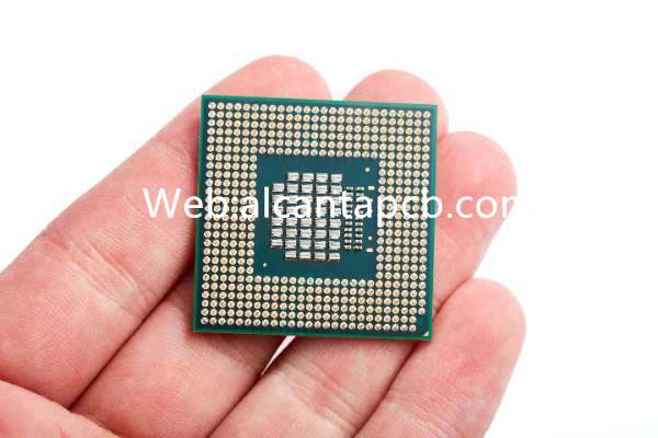
FC-BGA (Fine-Pitch Ball Grid Array) ambalajul este de înaltă densitate, tehnologie de ambalare de înaltă performanță în care minuscule bile de lipit sunt aranjate sub formă de grilă pentru a conecta cipurile și plăcile de circuite imprimate (PCB -uri). Este de obicei folosit în dispozitive electronice cu integrare ridicată și dimensiuni reduse ale pachetului, oferind performanță și fiabilitate mai bune.
Care este diferența dintre substratul de ambalare ultra-multistrat FC-BGA și placa de circuit tradițională?
Substratul de ambalare ultra-multistrat FC-BGA utilizează tehnologia de stivuire multistrat, care are o densitate mai mare a circuitelor și integrare a componentelor decât plăcile de circuite tradiționale. În plus, are avantajele unei interferențe electromagnetice mai mici, fiabilitate mai mare și dimensiunea pachetului mai compactă.
Pentru ce domenii sunt potrivite substraturile de ambalare FC-BGA ultra-multistrat?
Substratul de ambalare ultra-multistrat FC-BGA este utilizat pe scară largă în echipamentele de comunicații, electronice auto, Echipament medical, automatizări industriale și alte domenii. Sunt potrivite pentru aplicații care necesită performanțe ridicate, fiabilitate ridicată și ambalaj compact.
Care sunt avantajele substratului de ambalare ultra-multistrat FC-BGA?
Acest substrat de ambalare are avantajele densității mari, interferențe electromagnetice scăzute, fiabilitate ridicată și ambalaj compact. Ele îmbunătățesc performanța plăcii, economisiți spațiu, și asigură o funcționare stabilă pe termen lung.
Ce factori trebuie luați în considerare atunci când alegeți un substrat de ambalare FC-BGA super multi-strat?
Când selectați un substrat de ambalare FC-BGA super multi-strat, factori precum indicatorii săi de performanță, dimensiunea ambalajului, adaptabilitate la mediu, și reputația producătorului trebuie luată în considerare. Asigurați-vă că alegeți un produs care să corespundă nevoilor proiectului dumneavoastră și care are fiabilitate garantată.