CO., LTD")
Producător de substraturi BGA pentru procesoare ultra-subțiri.”Producător de substraturi BGA pentru procesoare ultra-subțiri” se referă la o companie specializată în producția de matrice ultra-subțire Ball Grid (BGA) substraturi pentru procesoare. Ei se concentrează pe crearea subțiri, soluții de interconectare de înaltă densitate care îmbunătățesc performanța și eficiența dispozitivelor electronice.
În tehnologia electronică modernă, CPU ultra-subțire Substraturi BGA sunt una dintre componentele cheie. Nu numai că excelează în performanță și dimensiune, ele promovează, de asemenea, miniaturizarea și eficiența ridicată a dispozitivelor electronice. Acest articol va explora în detaliu diferite aspecte ale acestor substraturi.
Ce sunt substraturi BGA pentru procesoare ultra-subțiri?
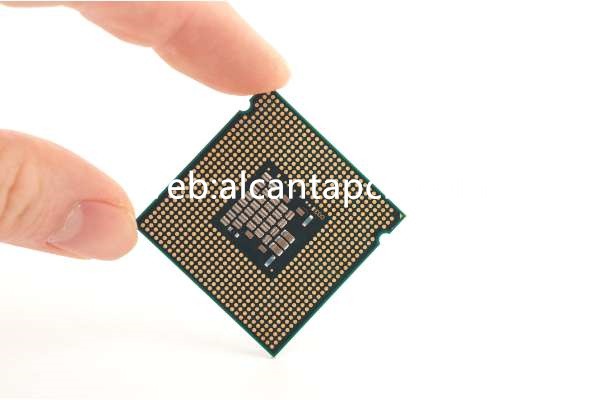
CPU BGA ultra-subțire Substraturi referiți-vă la matricea grilă cu bile ultra-subțiri (BGA) substraturi utilizate pentru conectarea și susținerea unității centrale de procesare (CPU) și alte componente electronice. Acest substrat nu transportă doar procesorul, dar oferă și transmisie de semnal și distribuție a puterii prin circuite și cablaje sofisticate. Caracteristica sa principală este grosimea sa extrem de subțire, de obicei între câteva sute de microni și câțiva milimetri.
Aceste substraturi joacă un rol vital în dispozitivele electronice moderne. Pe măsură ce cerințele de performanță ale dispozitivului cresc și dimensiunile scad, substraturile cu grosimi tradiționale nu mai sunt capabile să îndeplinească cerințele de înaltă densitate și de înaltă performanță. Substraturile ultra-subțiri pot oferi performanțe electrice mai mari și eficiență de disipare a căldurii prin reducerea grosimii și optimizarea materialelor și a designului.
Designul substraturilor BGA pentru procesoare ultra-subțiri trebuie să ia în considerare mai mulți factori. Prima este selecția materialului, care utilizează de obicei rășini organice de mare densitate, ceramica si materiale metalice. Aceste materiale nu trebuie doar să aibă o conductivitate electrică bună, dar și să poată lucra stabil în medii cu temperatură ridicată. Al doilea este rezistența mecanică și durabilitatea. Este necesar un design ultra-subțire pentru a se asigura că substratul nu va eșua din cauza solicitărilor mecanice în timpul utilizării pe termen lung. În plus, performanța electrică este, de asemenea, cheia, și designerii trebuie să se asigure că substratul poate oferi o cale de rezistență scăzută și conductivitate ridicată pentru a asigura stabilitatea și fiabilitatea transmisiei semnalului.
În aplicații practice, Substratele BGA ultra-subțiri ale procesorului nu numai că îmbunătățesc performanța dispozitivului, dar și reduce semnificativ dimensiunea și greutatea dispozitivului. Acest lucru este important în special pentru dispozitivele portabile, cum ar fi smartphone-urile, tablete, si laptopuri. Aceste dispozitive au cerințe stricte pentru portabilitate și durata de viață a bateriei, și substraturile ultra-subțiri îndeplinesc aceste nevoi prin performanța și designul lor excelent.
Substraturile ultra-subțiri prezintă, de asemenea, un potențial mare în calculul de înaltă performanță. Echipamente precum servere, centre de date, iar acceleratoarele de inteligență artificială trebuie să proceseze cantități mari de date și sarcini complexe de calcul, și au cerințe extrem de ridicate privind performanța electrică și capacitățile de disipare a căldurii ale substratului. Substraturile BGA ultra-subțiri ale procesorului pot îmbunătăți eficient eficiența și fiabilitatea acestor dispozitive prin conductivitate ridicată și disipare ridicată a căldurii.
În plus, progresează și fabricarea de substraturi ultra-subțiri. Procesele și tehnologiile avansate de fabricație fac ca producția de substraturi ultra-subțiri să fie mai precisă și mai eficientă. De exemplu, Tehnologiile de tăiere cu laser și microprelucrare pot atinge o precizie de fabricație extrem de ridicată și pot asigura consistența și stabilitatea microstructurii substratului. În același timp, introducerea liniilor de producție automatizate a îmbunătățit mult eficiența producției și randamentul, costuri de producție reduse, și a permis utilizarea substraturilor ultra-subțiri în mai multe domenii.
În general, Substraturile BGA ultra-subțiri ale procesorului sunt o forță motrice importantă pentru dezvoltarea tehnologiei electronice moderne. Prin designul lor unic și performanța excelentă, aceste substraturi nu numai că îmbunătățesc performanța generală a dispozitivului, dar promovează și miniaturizarea și performanța ridicată a dispozitivelor electronice. Cu progresul și inovarea continuă a tehnologiei, substraturile ultra-subțiri vor avea aplicații mai largi și performanțe mai mari în viitor.
Ghid de referință pentru proiectarea substraturilor BGA pentru procesoare ultra-subțiri
Proiectarea substraturilor BGA pentru procesoare ultra-subțiri (substraturi BGA ultra-subțiri ale procesorului) este o sarcină complexă și delicată care necesită respectarea unei serii de linii directoare și standarde stricte de proiectare. Aceste linii directoare nu acoperă doar selecția materialelor, proiectare mecanică, proiectare electrică, etc., dar implică şi procese de producţie, testarea si controlul calitatii. Mai jos sunt câteva linii directoare cheie de referință pentru proiectarea substraturilor BGA pentru procesoare ultra-subțiri.
În primul rând, selecția materialului este baza designului. Substratele BGA ultra-subțiri ale procesorului folosesc de obicei rășini organice de înaltă densitate (cum ar fi FR-4), ceramica si materiale metalice. FR-4 este utilizat pe scară largă datorită proprietăților sale mecanice bune și proprietăților de izolare electrică. Materiale ceramice, cu conductivitatea lor termică excelentă și stabilitatea la temperaturi ridicate, sunt potrivite pentru aplicații cu performanțe ridicate și cerințe ridicate de disipare a căldurii. În plus, pentru a îmbunătăți performanța conductivă a substratului, un strat de cupru sau alte materiale conductoare este de obicei placat pe și în interiorul substratului.
În al doilea rând, grosimea și numărul de straturi ale substratului trebuie optimizate în funcție de cerințele specifice de aplicare. Cheia pentru designul ultra-subțire este găsirea punctului favorabil dintre performanță și cost. Un substrat prea subțire poate duce la o rezistență mecanică insuficientă, în timp ce un substrat prea gros nu poate satisface nevoile de miniaturizare și integrare de înaltă densitate. Proiectanții trebuie să determine grosimea și numărul de straturi cele mai potrivite prin calcule și simulări precise.
În ceea ce privește aspectul și designul cablajului, un aspect rezonabil poate reduce interferența semnalului și poate îmbunătăți performanța generală a sistemului. Proiectanții trebuie să se asigure că lungimile traseului semnalului sunt menținute la minimum și să evite curbele și treceri inutile.. În plus, De asemenea, trebuie luate în considerare proiectarea sursei de alimentare și a firelor de împământare pentru a asigura stabilitatea sursei de alimentare și capacitatea anti-interferență a sistemului. Pentru procesarea semnalului de înaltă frecvență, proiectanții trebuie să acorde o atenție deosebită potrivirii impedanței și proiectării de ecranare a urmelor pentru a reduce reflexia semnalului și pierderile de radiație.
Pentru a asigura acuratețea și fiabilitatea proiectelor, designerii folosesc de obicei instrumente avansate de proiectare și software de simulare. Aceste instrumente pot simula comportamentul substraturilor în diferite condiții de operare, ajutând proiectanții să identifice și să rezolve probleme potențiale. De exemplu, Software-ul de simulare electromagnetică poate simula transmisia de semnale pe un substrat și poate analiza posibile interferențe și pierderi. Software-ul de simulare termică poate simula distribuția căldurii a substratului și poate ajuta proiectanții să optimizeze proiectarea disipării căldurii.
După finalizarea proiectării, sunt necesare o serie de teste și verificări pentru a se asigura că performanța reală a substratului îndeplinește cerințele de proiectare. Metodele obișnuite de testare includ testarea performanței electrice, testarea rezistenței mecanice, testarea ciclului termic, etc.. Aceste teste pot identifica potențiale probleme cu substratul în utilizare reală și pot asigura că poate funcționa stabil în diferite condiții de funcționare.
În cele din urmă, controlul calității este, de asemenea, o parte importantă a procesului de proiectare. Controlul strict al calității asigură performanța și fiabilitatea fiecărui substrat. Designerii trebuie să dezvolte standarde și procese detaliate de control al calității, inclusiv inspecția materialelor, controlul procesului de producție, inspecția produsului finit, etc.. Prin controlul cuprinzător al calității, rata defectelor de producție poate fi mult redusă și calitatea generală a produsului poate fi îmbunătățită.
În scurt, Proiectarea substraturilor BGA pentru procesoare ultra-subțiri este o sarcină complexă care necesită o luare în considerare cuprinzătoare a mai multor factori. Din selecția materialului, proiectare mecanică până la performanța electrică și managementul termic, fiecare legătură necesită un design meticulos și un control strict. Urmând o serie de linii directoare și standarde de proiectare, designerii pot dezvolta substraturi ultra-subțiri cu performanțe excelente și fiabilitate ridicată, oferind un sprijin puternic pentru dezvoltarea dispozitivelor electronice moderne.
Ce material este folosit în substraturi BGA pentru procesoare ultra-subțiri?
Substraturile BGA ultra-subțiri ale procesorului folosesc o varietate de materiale de înaltă performanță. Selectarea și aplicarea acestor materiale au un impact crucial asupra performanței, fiabilitatea și procesul de fabricație al substratului. Următoarele sunt câteva materiale utilizate în mod obișnuit și aplicațiile și caracteristicile acestora în substraturi BGA pentru procesoare ultra-subțiri.
În primul rând, materialele de rășină organică, cum ar fi FR-4, sunt cele mai comune materiale substrat. FR-4 este un material de rășină epoxidice armată cu fibră de sticlă, cu rezistență mecanică excelentă și proprietăți de izolare electrică.. Nu este doar rezistent la căldură și coroziune chimică, dar oferă și performanțe electrice stabile, deci este utilizat pe scară largă în fabricarea de substrat a diferitelor produse electronice. Pentru substraturi BGA pentru procesoare ultra-subțiri, FR-4 poate reduce și mai mult grosimea, menținând în același timp performanța mecanică și electrică prin formulare și proces îmbunătățite.
Materialele ceramice sunt, de asemenea, o alegere importantă în substraturile BGA pentru procesoare ultra-subțiri. Materialele ceramice utilizate în mod obișnuit includ oxidul de aluminiu (Al2O3) și nitrură de aluminiu (Aln). Aceste materiale au o conductivitate termică extrem de ridicată și proprietăți de izolare electrică, și poate funcționa stabil în medii cu temperaturi ridicate. Oxidul de aluminiu are proprietăți mecanice bune și este rentabil, în timp ce nitrura de aluminiu este potrivită pentru aplicații mai solicitante datorită conductivității termice și proprietăților electrice mai mari. În proiectarea substraturilor ultra-subțiri, Materialele ceramice pot îmbunătăți eficient capacitatea de disipare a căldurii a substratului și pot asigura funcționarea stabilă a procesorului.
Materiale metalice, precum cuprul și aliajele de cupru, sunt utilizate în principal pentru straturile conductoare și straturile de disipare a căldurii în substraturi BGA ultra-subțiri ale procesorului. Cuprul are o conductivitate electrică și termică excelentă și poate conduce eficient semnalele electrice și disipa căldura. În fabricarea substratului, procesele de galvanizare și gravare sunt adesea folosite pentru a forma modele conductoare precise pe și în interiorul substratului. Pentru aplicații de înaltă performanță, Aliajele de cupru pot fi, de asemenea, utilizate pentru a îmbunătăți rezistența mecanică și rezistența la oboseală a cuprului prin introducerea de elemente de aliere.
În ultimii ani, noi materiale, cum ar fi grafenul, au început să fie, de asemenea, utilizate în substraturi BGA pentru procesoare ultra-subțiri. Grafenul este un material bidimensional compus dintr-un singur strat de atomi de carbon care are o conductivitate electrică extrem de ridicată., conductivitate termică și rezistență mecanică. Proprietățile sale fizice și chimice unice conferă grafenului un mare potențial de aplicare pe substraturi ultra-subțiri. De exemplu, prin adăugarea de grafen la materialul substratului, conductivitatea termică și performanța electrică a substratului pot fi îmbunătățite semnificativ, grosimea poate fi redusă, iar rezistența mecanică poate fi îmbunătățită.
În plus, pentru a îmbunătăți în continuare performanța și fiabilitatea substratului, designerii vor folosi o varietate de materiale și structuri compozite. De exemplu, prin combinarea unui material de rășină organică cu o pulbere ceramică, se poate obține un substrat care are atât flexibilitatea materialului organic, cât și conductivitatea termică ridicată a materialului ceramic.. În mod similar, prin proiectarea structurală cu mai multe straturi, avantajele diferitelor materiale pot fi integrate în substrat, cum ar fi utilizarea de materiale foarte conductoare în stratul exterior și materiale de înaltă rezistență în stratul mijlociu, atingând astfel cel mai bun echilibru de performanță.
La selectarea și aplicarea acestor materiale, trebuie luați în considerare mai mulți factori, inclusiv proprietățile mecanice ale materialului, Proprietăți electrice, conductivitate termică, cost, și tehnici de prelucrare. De exemplu, pentru aplicații care necesită conductivitate termică și fiabilitate ridicate, cum ar fi centrele de calcul și de date de înaltă performanță, Pot fi preferate materiale de înaltă performanță precum ceramica și grafenul. Pentru electronice de larg consum, puteți lua în considerare costul și procesabilitatea mai mult și puteți alege materiale de rășină organică optimizate.
În general, Selectarea materialelor pentru substraturi BGA pentru procesoare ultra-subțiri este un proces complex și critic. Prin selectarea și combinarea rațională a diverselor materiale de înaltă performanță, substratul poate atinge cele mai bune performanțe din punct de vedere al rezistenței mecanice, performanta electrica, și managementul termic, satisfacând astfel nevoile diverselor dispozitive electronice high-end.
Ce dimensiune sunt substraturile BGA pentru procesoare ultra-subțiri?
Dimensiunea și forma substraturilor BGA ultra-subțiri ale procesorului (substraturi BGA ultra-subțiri ale procesorului) variază în funcție de nevoile aplicației. Grosimea, lungimea și lățimea acestor substraturi trebuie personalizate în funcție de pachetul CPU specific și mediul de aplicație. Următoarea este o discuție detaliată a designului de dimensiune a substraturilor BGA pentru procesoare ultra-subțiri.
Primul, grosimea substratului este un parametru critic. De obicei, grosimea substraturilor BGA ultra-subțiri pentru procesoare variază de la câteva sute de microni la câțiva milimetri. Alegerea grosimii specifice depinde de o varietate de factori, inclusiv rezistența mecanică, proprietăți electrice și capacități de disipare a căldurii. Pentru dispozitive portabile, precum smartphone-uri și tablete, designerii tind adesea să aleagă substraturi cât mai subțiri posibil pentru a reduce dimensiunea și greutatea totală a dispozitivului. Cu toate acestea, un substrat prea subțire poate duce la o rezistență mecanică insuficientă și se poate îndoi sau rupe cu ușurință în timpul utilizării. Prin urmare, în timpul procesului de proiectare, este necesar să se găsească cel mai bun punct de echilibru între grosime și rezistență prin calcul și simulare precise.
După determinarea grosimii substratului, lungimea și lățimea substratului trebuie, de asemenea, proiectate în funcție de aplicația specifică. Diferitele dimensiuni ale pachetului CPU și cerințele de aspect vor afecta dimensiunile generale ale substratului. În general vorbind, lungimea și lățimea substratului ar trebui să poată acoperi complet pachetul procesorului și alte componente electronice necesare, și rezervați spațiu adecvat pentru cablarea semnalului și distribuția energiei. În plus, forma substratului trebuie, de asemenea, să se potrivească cu designul extern al dispozitivului pentru a asigura o potrivire strânsă cu alte componente în timpul asamblarii.
Pentru a îmbunătăți flexibilitatea și adaptabilitatea designului, designul de dimensiune a substraturilor BGA pentru procesoare ultra-subțiri adoptă de obicei o abordare modulară și personalizată. Designul modular permite proiectanților să selecteze și să combine module de plinte de diferite dimensiuni și forme, în funcție de nevoile diferitelor aplicații, pentru a obține performanțe optime și rentabilitate.. Designul personalizat se bazează pe nevoile speciale ale proiectelor specifice, cu dimensiuni și design specializate pentru a îndeplini cerințele aplicațiilor specifice.
Densitatea cablurilor este, de asemenea, un aspect important în dimensionare. Pe măsură ce funcționalitatea dispozitivelor electronice continuă să crească, la fel și numărul de componente electronice și puncte de conectare de pe substrat. Proiectanții trebuie să dispună în mod rezonabil aceste componente și puncte de conectare pe o zonă limitată de substrat pentru a asigura stabilitatea transmisiei semnalului și fiabilitatea distribuției de energie.. În acest scop, Tehnologia de cablare avansată și instrumente de proiectare trebuie utilizate pentru a îmbunătăți densitatea cablajului și integrarea substratului prin optimizarea căilor de cablare și a conexiunilor între straturi..
În plus, designul dimensiunii substratului trebuie să ia în considerare și procesul de producție și costul. Designul dimensional prea complex și precis poate crește dificultatea de producție și costul, afectând economia produsului final. Designerii trebuie să găsească cel mai bun echilibru între performanță și cost prin optimizarea proceselor și controlul costurilor. De exemplu, în timpul procesului de proiectare, dimensiunile și șabloanele standardizate pot fi utilizate pentru a reduce complexitatea și variabilitatea procesului de producție și pentru a îmbunătăți eficiența producției și randamentul.
În aplicațiile reale, designul de dimensiune a substraturilor BGA pentru procesoare ultra-subțiri necesită încă o serie de teste și verificări. Prin fabricarea și testarea probelor fizice, pot fi verificate fezabilitatea și fiabilitatea proiectării, iar potenţialele probleme pot fi descoperite şi rezolvate. Metodele obișnuite de testare includ testarea rezistenței mecanice, testarea performanței electrice, testarea ciclului termic, etc.. Aceste teste pot asigura performanța și fiabilitatea substratului în utilizare reală și pot satisface nevoile diferitelor condiții de funcționare.
În general, designul de dimensiune a substraturilor BGA pentru procesoare ultra-subțiri este un proces complex și critic care necesită o luare în considerare cuprinzătoare a mai multor factori, cum ar fi performanța mecanică, performanta electrica, capacitatea de disipare a căldurii, procesul de producție și cost. Prin design de dimensiuni rezonabile, echilibrul optim de performanță și economie a substratului poate fi atins pentru a satisface nevoile diverselor dispozitive electronice de ultimă generație.
Procesul de fabricație al substraturilor BGA pentru procesoare ultra-subțiri
Procesul de fabricație a substraturilor BGA pentru procesoare ultra-subțiri (substrat ultra-subțire pentru CPU BGA) este complex și precis și necesită mai multe procese pentru a fi finalizat. Fiecare proces necesită un control strict și optimizare pentru a asigura calitatea și performanța produsului final. Mai jos este o descriere detaliată a procesului de fabricație a substraturilor BGA pentru procesoare ultra-subțiri.
Primul este selectarea și pregătirea materialelor de substrat. Conform cerințelor de proiectare, selectați rășina organică adecvată, materiale ceramice sau metalice. Alegerea materialului trebuie să ia în considerare nu numai proprietățile sale mecanice și electrice, dar și performanța de prelucrare și costul acesteia. După ce materialul este selectat, tăierea și modelarea sunt necesare pentru a tăia bucata mare de material într-un semifabricat de substrat de dimensiunea și forma specificate. Acest proces utilizează de obicei echipamente de tăiere de înaltă precizie, precum tăietoarele cu laser sau tăietoarele CNC, pentru a asigura acuratețea și consistența dimensiunilor substratului.
Urmează procesul de laminare și laminare. Pentru modele de substrat cu mai multe straturi, mai multe straturi de materiale trebuie să fie stivuite împreună și presate prin temperatură ridicată și presiune ridicată pentru a forma un substrat compozit cu căi conductoare multistrat. În timpul procesului de laminare, temperatură, presiunea și timpul trebuie controlate strict pentru a asigura o legătură strânsă și conexiunea electrică între diferitele straturi de materiale. Acest proces se realizează de obicei într-un mediu de vid pentru a evita introducerea de aer și impurități, ceea ce poate afecta performanța și fiabilitatea substratului.
După ce laminarea este finalizată, substratul trebuie să fie găurit și galvanizat. Procesul de găurire este utilizat pentru a crea căi de conectare electrică, precum găurile traversante și găurile oarbe, pe substrat. Acest proces utilizează de obicei echipamente de foraj de înaltă precizie, fie prin găurire mecanică, fie prin găurire cu laser, pentru a asigura acuratețea locației și dimensiunii găurilor. Procesul de galvanizare acoperă un strat de cupru sau alte materiale conductoare pe suprafața substratului și pe pereții găurilor pentru a forma căi de conectare electrică. Acest proces trebuie desfășurat sub parametri stricti de proces pentru a asigura grosimea și uniformitatea acoperirii.
Aceasta este urmată de procese de fotolitografie și gravare. Procesul de fotolitografie folosește tehnologia fotolitografiei pentru a forma modelul de circuit necesar pe suprafața substratului. Primul, un strat de material fotosensibil este acoperit pe suprafața substratului, iar apoi modelul este expus pe materialul fotosensibil printr-o fotomască. După expunere, porţiunea fotosensibilă a materialului fotosensibil este dizolvată de revelator, lăsând modelul dorit. Procesul de gravare folosește un agent chimic pentru a îndepărta materialul în exces, lăsând o cale conductivă protejată de materialul fotosensibil. Acest proces necesită un control strict al timpului de gravare și al concentrației de gravare pentru a asigura acuratețea modelului și integritatea traseului conductiv.
După ce fotolitografia și gravura sunt finalizate, substratul trebuie de asemenea să fie supus unei serii de curățare, procese de testare și ambalare. Procesul de curățare este utilizat pentru a îndepărta reziduurile și contaminanții de pe suprafața substratului pentru a asigura curățenia și performanța substratului. Procesul de testare verifică performanța și fiabilitatea substratului prin testarea performanței electrice, testarea rezistenței mecanice, testarea ciclului termic și alte metode. Procesul de ambalare asamblează substratul și alte componente electronice împreună pentru a forma un modul sau dispozitiv electronic complet.
Pentru a asigura stabilitatea procesului de fabricatie si calitatea produselor, producătorii adoptă de obicei echipamente avansate de producție și sisteme de control al proceselor. De exemplu, liniile de producție automatizate pot îmbunătăți eficiența și consistența producției și pot reduce erorile și variabilitatea cauzate de operațiuni manuale. Sistemul de detectare și monitorizare online poate monitoriza parametrii cheie din procesul de producție în timp real, descoperiți și corectați potențialele probleme în timp util, și să asigure calitatea și stabilitatea fiecărui proces.
În plus, optimizarea și îmbunătățirea proceselor de producție sunt, de asemenea, modalități importante de îmbunătățire a calității produselor și de reducere a costurilor de producție. Prin îmbunătățirea continuă a proceselor și inovarea tehnologică, eficiența de fabricație și performanța produsului pot fi îmbunătățite, iar costurile de producție și ratele de deșeuri pot fi reduse. De exemplu, folosind materiale și procese mai eficiente, optimizarea fluxurilor și parametrilor procesului, și aplicarea tehnologiilor avansate de detectare și control sunt toate mijloace importante pentru optimizarea procesului de fabricație.
În general, procesul de fabricație a substraturilor BGA pentru procesoare ultra-subțiri este complex și precis, care necesită o analiză cuprinzătoare a selecției materialelor, controlul procesului, aplicarea echipamentelor, si managementul calitatii. Prin control strict și optimizare continuă, calitatea și performanța produsului final pot fi asigurate pentru a satisface nevoile diverselor echipamente electronice de ultimă generație.
Zona de aplicare a substraturilor BGA pentru procesoare ultra-subțiri
Substraturi BGA pentru procesoare ultra-subțiri (substraturi BGA ultra-subțiri ale procesorului) au o gamă largă de aplicații. Performanța lor excelentă și designul ultra-subțire le fac utilizate pe scară largă în echipamentele electronice moderne. Mai jos sunt câteva domenii principale de aplicare și exemple specifice.
Primul, Substratele BGA ultra-subțiri ale procesorului sunt utilizate pe scară largă în dispozitivele electronice portabile, cum ar fi smartphone-urile și tabletele. Aceste dispozitive au restricții stricte privind dimensiunea și greutatea. Substraturile ultra-subțiri pot reduce semnificativ grosimea și greutatea totală a dispozitivului, îmbunătățind în același timp performanța și fiabilitatea dispozitivului.. În smartphone-uri, substraturi ultra-subțiri sunt folosite pentru a transporta și conecta procesoarele, GPU-uri și alte cipuri cheie, oferind transmisie eficientă a semnalului și distribuție a puterii. În tablete, substratul ultra-subțire ajută dispozitivul să rămână rece în timpul funcționării de înaltă performanță și prelungește durata de viață a dispozitivului prin performanța sa excelentă de disipare a căldurii.
În plus, Substraturile BGA ale procesorului ultra-subțiri sunt, de asemenea, utilizate în dispozitive de calcul portabile, cum ar fi computerele notebook și ultrabook-urile. În timp ce aceste dispozitive urmăresc performanțe ridicate, au, de asemenea, cerințe stricte pentru portabilitate și durata de viață a bateriei. Prin conductivitate ridicată și disipare ridicată a căldurii, substraturile ultra-subțiri pot reduce grosimea și greutatea dispozitivului, asigurând în același timp performanța dispozitivului, și îmbunătățiți experiența utilizatorului. În computerele notebook de înaltă performanță, substraturile ultra-subțiri sunt folosite pentru a conecta și susține componente cheie, cum ar fi procesorul, GPU și memorie, oferind soluții eficiente de distribuție a energiei și răcire.
Pe lângă dispozitivele portabile, Substratele BGA pentru procesoare ultra-subțiri sunt, de asemenea, utilizate pe scară largă în domeniul calculului de înaltă performanță. De exemplu, serverele și centrele de date trebuie să proceseze cantități mari de date și sarcini complexe de calcul, și au cerințe extrem de ridicate privind performanța electrică și capacitățile de disipare a căldurii ale substratului. Substraturile BGA ultra-subțiri ale procesorului pot îmbunătăți eficiența și stabilitatea de calcul în servere și centre de date prin performanța lor electrică excelentă și conductivitate termică ridicată. În acceleratoare de inteligență artificială și computere de înaltă performanță, Substraturile ultra-subțiri asigură transmisie eficientă a semnalului și distribuție a puterii prin cablarea lor de înaltă densitate și conductivitate ridicată, sprijinirea sarcinilor complexe de calcul și procesare a datelor.
Substratele CPU BGA ultra-subțiri sunt, de asemenea, utilizate pe scară largă în dispozitivele portabile și dispozitivele IoT. Aceste dispozitive sunt de obicei mici și ușoare și au cerințe stricte privind dimensiunea substratului și performanța. Substraturile ultra-subțiri pot satisface nevoile dispozitivelor purtabile și IoT prin designul lor miniaturizat și materialele de înaltă performanță. În ceasurile inteligente, dispozitive de monitorizare a sănătății și dispozitive smart home, substraturile ultra-subțiri asigură transmisie eficientă a semnalului și gestionarea puterii prin integrarea lor ridicată și fiabilitatea ridicată, sprijinirea implementării diverselor funcții inteligente.
În plus, Substraturile BGA ultra-subțiri ale procesorului sunt, de asemenea, utilizate pe scară largă în domeniul electronicii auto și al controlului industrial.. În electronica auto, substraturile ultra-subțiri sunt folosite pentru a conecta și susține diverși senzori, controlere și module de comunicație, asigură transmisie eficientă a semnalului și distribuție a puterii, și suportă funcții avansate, cum ar fi conducerea autonomă și Internetul vehiculelor. În echipamentele de control industrial, substraturile ultra-subțiri suportă sarcini complexe de control și procesare a datelor, îmbunătățirea eficienței producției și a stabilității sistemului prin fiabilitatea și performanța lor ridicată.
În general, Substratele CPU BGA ultra-subțiri sunt utilizate pe scară largă în dispozitivele electronice moderne. Performanța lor excelentă și designul ultra-subțire le fac utilizate pe scară largă în smartphone-uri, tablete, laptopuri, echipamente de calcul de înaltă performanță, Dispozitive purtabile, A fost utilizat pe scară largă în domenii precum dispozitivele IoT, electronică auto și control industrial. Prin inovarea tehnologică continuă și extinderea aplicațiilor, Substratele ultra-subțiri ale procesorului BGA vor juca un rol mai important în viitor și vor promova progresul și dezvoltarea tehnologiei electronice.
Care sunt avantajele substraturilor BGA pentru procesoare ultra-subțiri?
Substraturi BGA pentru procesoare ultra-subțiri (substraturi BGA ultra-subțiri ale procesorului) au multe avantaje datorită designului lor unic și performanței excelente. Iată o privire mai atentă asupra principalelor sale beneficii.
Primul, unul dintre cele mai mari avantaje ale substraturilor BGA pentru procesoare ultra-subțiri este designul lor ultra-subțire. Acest design poate reduce semnificativ dimensiunea și greutatea totală a dispozitivelor electronice, care este deosebit de important pentru dispozitivele portabile, cum ar fi smartphone-urile, tablete si laptopuri. Ca consumatori’ cererile de portabilitate și ușurință continuă să crească, substraturile ultra-subțiri ajută producătorii de echipamente să obțină produse mai ușoare și mai subțiri prin design-urile lor miniaturizate, imbunatatind astfel competitivitatea pietei.
În al doilea rând, Substraturile CPU BGA ultra-subțiri folosesc de obicei materiale de înaltă performanță, cu proprietăți excelente de conductivitate electrică și de disipare a căldurii. Aceste materiale includ rășini organice de înaltă densitate, ceramică și materiale metalice precum cuprul și aliajele de cupru. Materialele foarte conductoare pot oferi căi electrice cu rezistență scăzută și conductivitate ridicată pentru a asigura stabilitatea și fiabilitatea transmisiei semnalului. Materialele cu conductivitate termică ridicată pot disipa eficient căldura, reduce temperatura de funcționare a componentelor electronice, și extinde durata de viață a echipamentelor. În aplicații de înaltă performanță, precum servere și centre de date, performanța ridicată de disipare a căldurii a substraturilor ultra-subțiri este deosebit de importantă. Poate ajuta echipamentele să mențină temperaturi scăzute în timpul operațiunilor cu sarcină mare și să îmbunătățească stabilitatea și eficiența sistemului.
În plus, capacitatea de cablare de înaltă densitate a substraturilor BGA pentru procesoare ultra-subțiri este, de asemenea, un avantaj major. Substraturile ultra-subțiri pot realiza un aspect de circuit de înaltă densitate și conexiuni pe o zonă limitată de substrat prin tehnologie de cablare avansată și instrumente de proiectare. Acest lucru nu permite doar integrarea mai multor module funcționale și componente electronice, îmbunătățirea integrării și funcționalității sistemului, dar, de asemenea, optimizează calea semnalului și reduce interferența și întârzierea semnalului. În smartphone-uri, tablete și dispozitive de calcul de înaltă performanță, capabilitățile de cablare de înaltă densitate pot îmbunătăți semnificativ performanța sistemului și experiența utilizatorului.
Substraturile ultra-subțiri au, de asemenea, proprietăți mecanice bune și durabilitate. În ciuda grosimii sale subțiri, prin selectarea materialelor de înaltă rezistență și optimizarea designului structural, substratul ultra-subțire poate oferi în continuare o rezistență mecanică suficientă pentru a rezista la diferite solicitări mecanice și vibrații. Acest lucru asigură că substratul nu este ușor deteriorat în timpul utilizării pe termen lung și menține funcționarea stabilă a echipamentului. În unele aplicații speciale, cum ar fi electronice auto și echipamente de control industrial, proprietățile mecanice și durabilitatea substraturilor ultra-subțiri sunt deosebit de importante, care poate îmbunătăți fiabilitatea și durata de viață a sistemului.
Eficiența costurilor este, de asemenea, un avantaj major al substraturilor BGA pentru procesoare ultra-subțiri. Deși procesul de fabricație a substraturilor ultra-subțiri este relativ complex, cu progresul continuu al tehnologiei și extinderea scarei de producție, costurile sale de producţie scad treptat. Prin optimizarea selecției materialelor, îmbunătățirea proceselor de producție și îmbunătățirea eficienței producției, producătorii pot reduce costurile de producție și pot îmbunătăți economia produsului. Acest lucru permite promovarea și aplicarea substraturilor ultra-subțiri în mai multe domenii de aplicare, promovând astfel popularizarea și dezvoltarea tehnologiei electronice.
În cele din urmă, flexibilitatea de aplicare a substraturilor BGA pentru procesoare ultra-subțiri este, de asemenea, unul dintre avantajele sale. Prin design modular și personalizat, substraturile ultra-subțiri se pot adapta la diferite nevoi de aplicare și medii. Fie că este vorba de smartphone -uri, tablete, laptopuri, servere, centre de date, Dispozitive purtabile, Dispozitive IoT, electronice auto și echipamente de control industrial, substraturile ultra-subțiri pot oferi cea mai bună performanță și soluție.
În general, Substraturile BGA ale procesorului ultra-subțiri au multe avantaje, inclusiv design ultra-subțire, materiale performante, capabilități de cablare de înaltă densitate, proprietăți mecanice bune și durabilitate, rentabilitatea și flexibilitatea aplicațiilor. Aceste avantaje îl fac să aibă perspective largi de aplicare și potențial de piață în echipamentele electronice moderne, promovarea progresului și dezvoltării continue a tehnologiei electronice.
FAQ
1. Care este grosimea tipică a substraturilor BGA pentru procesoare ultra-subțiri?
Grosimile tipice variază de la câteva sute de microni la câțiva milimetri, în funcție de necesitățile aplicației și cerințele de proiectare. Pentru dispozitive portabile precum smartphone-uri și tablete, cel mai subțire substrat posibil este adesea ales pentru a reduce dimensiunea și greutatea totală a dispozitivului.
2. Care sunt principalele materiale ale substraturilor ultra-subțiri?
Principalele materiale includ rășini organice (cum ar fi FR-4), ceramica si diverse materiale metalice, precum cuprul și aliajele de cupru. Uneori sunt adăugate materiale noi, cum ar fi grafenul, pentru a îmbunătăți și mai mult performanța substratului.
3. Este dificil să fabricați substraturi BGA pentru procesoare ultra-subțiri?
Fabricarea este dificilă și necesită procese multiple de precizie, inclusiv selecția și pregătirea materialelor, laminare și laminare, găurire și galvanizare, fotolitografia și gravura, curățare și testare, ambalaj, etc.. Fiecare proces necesită un control strict și optimizare pentru a asigura calitatea și performanța produsului final.
4. În ce domenii sunt utilizate în principal substraturi ultra-subțiri?
Folosit în principal în smartphone-uri, tablete, laptopuri, echipamente de calcul de înaltă performanță, Dispozitive purtabile, Echipamente pentru internetul obiectelor, electronice auto și echipamente de control industrial, etc.. Aceste aplicații impun cerințe stricte privind performanța substratului, dimensiune și fiabilitate.