CO., LTD")
Vipofu Vias&Kuzikwa Vias PCB Viwanda. Nafasi ndogo sana, ndogo sana kupitia mashimo ya HDI PCB. tunatoa Vias Vipofu vya hali ya juu&Kuzikwa Vias kutoka 4 Tabaka kwa 50 tabaka. wakati wa usafirishaji wa haraka. na ubora wa juu.
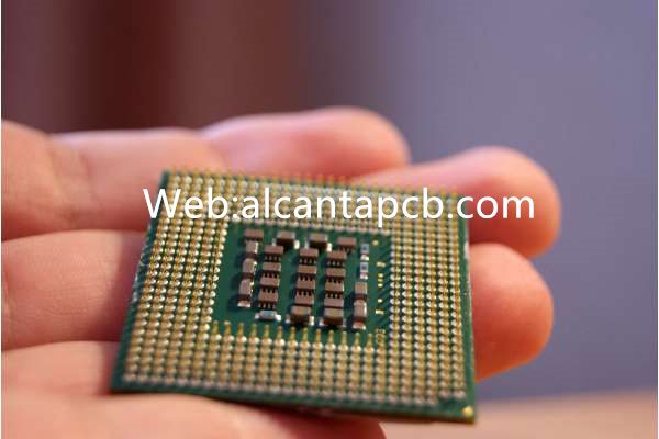
Katika PCB (Bodi ya Mzunguko Iliyochapishwa) Viwanda, upofu kupitia na kuzikwa kupitia teknolojia huchukua jukumu muhimu. Sio tu kwamba huongeza utendaji wa bodi na wiani, lakini pia zinaweza kusaidia kuwezesha miundo changamano zaidi. Makala haya yatajikita katika ufafanuzi, kanuni za kubuni, michakato ya utengenezaji, na maeneo ya matumizi ya teknolojia hizi, kukupa mwongozo wa kina ili kukusaidia kuelewa vyema na kutumia upofu na kuzikwa kupitia teknolojia.
Ni nini hasa ni vipofu kupitia na kuzikwa kupitia teknolojia?
Katika uwanja wa PCB (Bodi ya Mzunguko Iliyochapishwa) Viwanda, upofu kupitia na kuzikwa kupitia teknolojia ni michakato miwili muhimu. Wanacheza jukumu muhimu katika kuongeza wiani wa bodi za mzunguko, kupunguza ukubwa na kuboresha utendaji.
Kwanza kabisa, kipofu kupitia ni shimo ambalo linaundwa upande mmoja tu wa bodi ya mzunguko na haionekani kwa upande mwingine. Kuzikwa kupitia ni shimo ambalo hupenya bodi nzima ya mzunguko na haionekani kwa pande zote mbili. Aina zote mbili za shimo huundwa kwa kuchimba visima kwanza na kisha kujaza mashimo kwa chuma na kisha kuzijaza na nyenzo za kufunika uso ili shimo zisipenye bodi nzima ya mzunguko..
Umuhimu wa upofu kupitia na kuzikwa kupitia teknolojia katika muundo wa PCB unajidhihirisha. Kwanza, wanaweza kuongeza kwa ufanisi wiani wa bodi za mzunguko. Kwa kutumia vipofu na kuzikwa kupitia teknolojia katika PCB, wabunifu wanaweza kuingiza vipengele zaidi na waya kwenye nafasi ndogo, kusababisha muundo thabiti zaidi. Hii ni muhimu kwa miundo ndogo ambayo inahitaji ujumuishaji wa hali ya juu katika vifaa vya kisasa vya kielektroniki.
Pili, teknolojia hizi zinaweza kuboresha utendaji wa bodi za mzunguko. Kwa kupunguza urefu wa njia na upinzani wa maambukizi ya ishara, vias vipofu na kuzikwa vinaweza kuboresha kasi na uthabiti wa upitishaji wa mawimbi. Hii ni muhimu hasa katika programu zinazohusisha usambazaji wa mawimbi ya dijiti ya masafa ya juu na ya kasi ya juu, kama vile vifaa vya mawasiliano na mifumo ya kompyuta.
Aidha, shimo kipofu na teknolojia ya shimo la kuzikwa pia inaweza kuongeza kuegemea kwa bodi ya mzunguko. Kwa sababu wao hupunguza ukubwa na uzito wa bodi, wao hupunguza athari za mkazo wa mitambo na vibration kwenye ubao. Aidha, wanaweza kupunguza idadi ya pointi za solder kwenye bodi ya mzunguko, na hivyo kupunguza kiwango cha kushindwa kutokana na soldering duni.
Kukamilisha, upofu kupitia na kuzikwa kupitia teknolojia huchukua jukumu muhimu katika muundo wa PCB. Hawawezi tu kuboresha wiani na utendaji wa bodi za mzunguko, lakini pia kuongeza uaminifu wa bodi za mzunguko, hivyo kutoa msaada muhimu kwa ajili ya maendeleo ya vifaa vya kisasa vya elektroniki.
Jinsi ya kubuni PCB na Vipofu na kuzikwa vias?
Katika muundo wa PCB, vias vipofu na vias kuzikwa ni teknolojia ya kawaida, na zina jukumu muhimu katika kuboresha wiani wa bodi ya mzunguko na utendaji. Kubuni PCB zilizo na vias vipofu na kuzikwa kunahitaji kuzingatia mambo mengi, ikiwa ni pamoja na kanuni za kubuni, pointi muhimu, na mwingiliano na vipengele vingine. Hapo chini tutazame jinsi ya kuunda PCB yenye vias vipofu na kuzikwa.
Vipu vya upofu ni mashimo yaliyotobolewa upande mmoja wa bodi ya saketi hadi kina maalum bila kupitia unene mzima wa ubao.. Kanuni zake za kubuni ni pamoja na:
Nafasi na kupanga: Wakati wa awamu ya kubuni, kuamua eneo na idadi ya mashimo ya vipofu ili kuhakikisha wanaratibu na mpangilio wa vipengele vingine.
Uunganisho wa Interlayer: Mashimo ya kipofu hutumiwa kuanzisha uhusiano kati ya tabaka tofauti, kwa hivyo kipenyo cha shimo na kina kinahitaji kudhibitiwa kwa usahihi ili kuhakikisha kuegemea kwa upitishaji wa ishara.
Utendaji conductive: Utendaji wa conductive wa mashimo ya vipofu huathiri moja kwa moja utulivu na utendaji wa mzunguko, kwa hivyo inahitajika kuchagua nyenzo na michakato inayofaa kwa utengenezaji.
Vipu vilivyozikwa ni mashimo ambayo hupenya kabisa bodi ya mzunguko na kujazwa na chuma au vifaa vya kuhami. Kanuni zake za kubuni ni pamoja na:
Utendaji wa kuziba: Njia zilizozikwa zinahitaji kuwa na utendaji mzuri wa kuziba ili kuzuia mazingira ya nje kuathiri mzunguko, hivyo uteuzi wa vifaa vya kujaza na udhibiti wa mchakato unahitaji kuzingatiwa katika kubuni.
Uadilifu wa ishara: Vipu vilivyozikwa hutumiwa kuboresha utendaji na utulivu wa bodi za mzunguko, hivyo aperture na vifaa vya kujaza vinahitaji kudhibitiwa kwa usahihi ili kuhakikisha uadilifu wa maambukizi ya ishara.
Nguvu ya mitambo: Kupitia kuzikwa hucheza jukumu la usaidizi na muunganisho katika PCB, kwa hivyo ni muhimu kuhakikisha kuwa nyenzo za kujaza zina nguvu za kutosha za mitambo ili kuzuia kuvunjika au uharibifu wakati wa matumizi.
Kwa muhtasari, kubuni PCB yenye vias vipofu na kuzikwa kunahitaji uelewa wa kina wa kanuni zake za muundo na mambo muhimu, na mpangilio unaofaa na uteuzi wa nyenzo kulingana na mahitaji halisi ili kuhakikisha utendaji na utulivu wa bodi ya mzunguko.
Je, ni mchakato wa utengenezaji wa vias vipofu na vias kuzikwa?
Katika mchakato wa utengenezaji wa PCB (Bodi ya Mzunguko Iliyochapishwa), shimo kipofu na teknolojia ya shimo lililozikwa ni hatua muhimu, ambayo hutoa wiani wa juu na utendaji kwa bodi ya mzunguko. Ifuatayo itatoa muhtasari wa mchakato wa utengenezaji wa vias vipofu na kuzikwa na kutambulisha hatua muhimu.
Mchakato wa utengenezaji wa vias vipofu na vias kuzikwa ni mojawapo ya viungo muhimu katika utengenezaji wa PCB. Kusudi lake ni kuunda viwango tofauti vya njia za uunganisho ndani ya bodi ya mzunguko ili kutambua wiring na uunganisho wa nyaya ngumu. Kufanya mashimo haya kunahitaji mfululizo wa hatua nyeti za mchakato, ikiwa ni pamoja na uchomaji kemikali, kuchimba visima, electroplating na zaidi.
Maandalizi ya kubuni: Kabla ya kutengeneza vias vipofu na vias kuzikwa, kazi ya maandalizi ya kubuni inahitajika, ikiwa ni pamoja na kuamua eneo, saizi, safu na vigezo vingine vya mashimo, na kuziweka alama kwenye faili ya muundo.
Maandalizi ya bodi: Kwanza, chagua ubao unaofaa kwa vipofu na kuzikwa kupitia utengenezaji, na kufanya matibabu ya uso juu yake ili kuhakikisha kwamba taratibu zinazofuata zinaweza kuendelea vizuri.
Uundaji wa muundo wa etching: Hatua ya kwanza katika utengenezaji wa vias vipofu na kuzikwa ni kuunda muundo unaohitajika kwenye uso wa ubao kupitia etching ya kemikali.. Hatua hii kwa kawaida hutumia mchakato wa upigaji picha ili kuunda mifumo ya etching kupitia mpiga picha.
Kuchimba visima: Baada ya kuunda muundo wa etching, unahitaji kutumia mashine ya kuchimba visima kuchimba bodi ya mzunguko. Mashimo haya ya kuchimba yatapitia sehemu moja au zaidi ya ubao, kuunda sura ya awali ya vias vipofu na kuzikwa.
Mchakato wa kusafisha: Baada ya kuchimba visima kukamilika, bodi ya mzunguko inahitaji kusafishwa ili kuondoa uchafu na mabaki yanayotokana wakati wa mchakato wa kuchimba visima ili kuhakikisha ubora na usahihi wa mashimo..
Electroplating: Inayofuata, bodi ya mzunguko inahitaji kupitia mchakato wa electroplating ili kuunda safu ya conductive kwenye uso wa kuchimba. Hatua hii husaidia kuboresha upitishaji wa vias vipofu na kuzikwa na huongeza uimara wao.
Kujaza: Kwa kuzikwa vias, kwa kawaida ni muhimu kujaza bodi ya mzunguko na nyenzo za kuhami ili kuzuia tabaka za conductive ndani ya mashimo kutoka kwa kuunganisha kwa kila mmoja.. Uchaguzi na usindikaji wa vifaa vya kujaza unahitaji kuzingatia mahitaji maalum ya kubuni.
Matibabu ya uso: Hatimaye, baada ya kukamilisha utengenezaji wa vias vipofu na kuzikwa, bodi ya mzunguko inahitaji matibabu ya uso ili kuboresha upinzani wake wa kutu na kuonekana.
Kupitia hatua muhimu hapo juu, vipofu na kuzikwa kupitia mchakato wa utengenezaji umekamilika, kutoa usaidizi wa kuaminika kwa utendaji na msongamano wa PCB. Utumiaji wa teknolojia hizi huwezesha vifaa vya kisasa vya kielektroniki kufikia miundo bora zaidi na ngumu ili kukidhi mahitaji ya soko yanayokua..
Inaweza kupofusha kupitia na kuzikwa kupitia teknolojia kuboresha utendaji na msongamano wa PCB?
Katika uwanja wa PCB (Bodi ya Mzunguko Iliyochapishwa) Viwanda, upofu kupitia na kuzikwa kupitia teknolojia ni uvumbuzi muhimu. Hawawezi tu kuboresha utendaji wa PCB, lakini pia kuongeza msongamano wake na kutambua miundo tata zaidi ya mzunguko. Hapa ni kuangalia kwa karibu faida za teknolojia hizi na jinsi zinavyoweza kupunguza ukubwa wa bodi na uzito.
Kwanza, upofu kupitia na kuzikwa kupitia teknolojia huruhusu miunganisho changamano ya mzunguko katika PCB za tabaka nyingi. Njia ya jadi ya uunganisho wa shimo haifanyi kazi vizuri katika PCB za tabaka nyingi kwa sababu inahitaji kupenya tabaka zote., wakati kipofu kupitia na kuzikwa kupitia teknolojia inaweza kuunganisha mizunguko kwenye tabaka tofauti bila kupenya unene wa bodi nzima. Kwa njia hii, wabunifu wanaweza kuweka vipengele vingi vya mzunguko katika nafasi ndogo, kuongeza wiani wa PCB.
Pili, upofu kupitia na kuzikwa kupitia teknolojia inaweza kupunguza saizi na uzito wa bodi za saketi. Kwa sababu vias vipofu na kuzikwa huruhusu miunganisho ya mzunguko kufanywa kati ya tabaka tofauti, wabunifu wanaweza kupanga vipengele kwa ufanisi zaidi, na hivyo kupunguza ukubwa wa PCB. Aidha, kupunguza unene wa bodi na idadi ya tabaka inaweza kupunguza uzito wa jumla, ambayo ni muhimu sana kwa vifaa vyepesi vya elektroniki.
Aidha, shimo kipofu na teknolojia ya shimo kuzikwa inaweza kuboresha kuegemea na utulivu wa PCB. Miunganisho ya kitamaduni ya kuchomwa huathiriwa na mkazo wa joto na mtetemo, ambayo inaweza kusababisha muunganisho kulegea au kukatika. Shimo kipofu na teknolojia ya shimo iliyozikwa inaweza kuunda uhusiano wenye nguvu kati ya tabaka tofauti, kuboresha upinzani wa mtetemo na uimara wa PCB.
Hatimaye, upofu kupitia na kuzikwa kupitia teknolojia pia inaweza kuboresha utendakazi wa mzunguko. Kwa sababu miunganisho ya mzunguko ni ngumu zaidi na yenye nguvu, kasi na utulivu wa maambukizi ya ishara huboreshwa, na hivyo kuboresha utendaji wa kifaa kizima cha kielektroniki.
Kwa muhtasari, upofu na kuzikwa kupitia teknolojia huleta faida nyingi kwa muundo na utengenezaji wa vifaa vya kielektroniki kwa kuongeza msongamano wa PCB, kupunguza ukubwa na uzito, kuimarisha kuegemea, na kuboresha utendaji. Pamoja na maendeleo endelevu ya teknolojia, shimo kipofu na teknolojia ya shimo lililozikwa itaendelea kuwa na jukumu muhimu katika uwanja wa utengenezaji wa PCB na kukuza maendeleo na uvumbuzi wa vifaa vya elektroniki..
Katika nyanja gani ni vipofu kupitia na kuzikwa kupitia teknolojia zinazotumiwa sana?
Upofu kupitia na kuzikwa kupitia teknolojia huchukua jukumu muhimu katika utengenezaji wa vifaa vya kisasa vya kielektroniki, na hutumiwa sana katika nyanja nyingi tofauti, hasa katika vifaa vya elektroniki vya viwango vya juu, vifaa vya mawasiliano, na umeme wa magari. Maeneo haya ya maombi yameelezwa kwa kina hapa chini:
Vifaa vya elektroniki vya msongamano mkubwa kama vile simu mahiri, vidonge, kompyuta za mkononi, nk. haja ya kuunganisha idadi kubwa ya vipengele vya elektroniki katika nafasi ndogo. Upofu kupitia na kuzikwa kupitia teknolojia hufanya muundo wa PCB ushikamane zaidi na unaweza kufikia msongamano wa juu wa vipengele, na hivyo kufanya kifaa kuwa kidogo na nyepesi. Aidha, teknolojia hizi pia zinaweza kuboresha utendakazi na uthabiti wa bodi za saketi na kukidhi mahitaji ya utendaji na uaminifu wa vifaa vya kisasa vya hali ya juu vya elektroniki..
Katika uwanja wa vifaa vya mawasiliano, kama vile vituo vya msingi, Njia, vifaa vya mawasiliano ya nyuzi za macho, nk., shimo kipofu na teknolojia ya shimo la kuzikwa pia imetumika sana. Vifaa hivi vinahitaji upitishaji wa mawimbi ya kasi ya juu na thabiti, na upofu kupitia na kuzikwa kupitia teknolojia inaweza kupunguza kwa ufanisi urefu na kutolingana kwa njia za upitishaji wa mawimbi na kuboresha kutegemewa na kasi ya utumaji mawimbi.. Aidha, vias vipofu na via vya kuzikwa vinaweza pia kuboresha utendaji wa kifaa cha kusambaza joto na kuimarisha uthabiti na uimara wa kifaa..
Pamoja na maendeleo endelevu ya teknolojia ya elektroniki ya magari, idadi kubwa ya vifaa na mifumo ya umeme imeunganishwa kwenye magari ya kisasa, kama vile vitengo vya kudhibiti injini (Funika), mifumo ya burudani ya ndani ya gari, mifumo ya usalama, nk. Upofu kupitia na kuzikwa kupitia teknolojia inaweza kusaidia kufikia ujumuishaji wa viwango vya juu vya mifumo ya kielektroniki ya magari na kuboresha utendakazi na utendakazi wa vifaa vya kielektroniki vya magari.. Wakati wa mchakato wa kuendesha gari, teknolojia hizi pia zinaweza kuboresha upinzani wa vibration na upinzani wa joto la juu la vifaa vya elektroniki na kuhakikisha uendeshaji thabiti wa mfumo wa elektroniki wa magari..
Kukamilisha, vipofu kupitia na kuzikwa kupitia teknolojia vimetumika sana katika nyanja za vifaa vya elektroniki vya msongamano mkubwa, vifaa vya mawasiliano, na umeme wa magari. Wanatoa msaada muhimu wa kiufundi kwa ajili ya kubuni na utengenezaji wa vifaa vya kisasa vya kielektroniki na kukuza maendeleo endelevu ya teknolojia ya kielektroniki. maendeleo na maendeleo.
PCB iliyo na vipofu na kuzikwa inagharimu kiasi gani?
Gharama ni muhimu kuzingatia wakati wa kutengeneza PCB zilizo na vias vipofu na kuzikwa. Kuelewa sababu za gharama za teknolojia hizi na jinsi ya kukadiria gharama ni muhimu katika kupanga bajeti na kuchagua mtengenezaji sahihi..
Ili kukadiria gharama ya PCB iliyo na vias vipofu na kuzikwa, kwanza unahitaji kuzingatia mambo hapo juu na kuwasiliana na wazalishaji wanaowezekana. Hapa kuna hatua kadhaa za kukadiria gharama:
Makadirio ya gharama ya nyenzo: Jadili gharama ya vifaa vilivyochaguliwa na mtengenezaji, kwa kuzingatia vipengele kama vile ukubwa wa PCB, idadi ya tabaka, nk.
Tathmini ya utata wa muundo: Tathmini utata wa muundo wa PCB, pamoja na idadi ya tabaka, kipenyo cha shimo, nafasi ya shimo, nk., na kuamua gharama za ziada ambazo zinaweza kufanywa na muundo.
Mchakato wa uteuzi na nukuu: Wasiliana na wazalishaji kuhusu mtiririko unaohitajika wa mchakato, ikijumuisha mahitaji maalum ya vipofu kupitia na kuzikwa kupitia teknolojia, na kukusanya nukuu kutoka kwa wazalishaji.
Athari ya wingi wa agizo: Kuzingatia athari za kiasi cha agizo kwenye gharama, jaribu kuchagua kiasi kinachofaa cha agizo ili kupata bei nzuri zaidi.
Mambo Mengine ya Gharama: Fikiria mambo mengine kama vile usafirishaji, kodi, na uwezekano wa huduma za ziada ili kutathmini kikamilifu gharama.
Kwa kuzingatia mambo yaliyo hapo juu na kulinganisha na wazalishaji wengi, unaweza kukadiria kwa usahihi zaidi gharama ya PCB zilizo na vias vipofu na kuzikwa na kuunda bajeti inayofaa.
Jinsi ya kuchagua mtengenezaji sahihi kwa utengenezaji wa PCB zilizo na vias vipofu na kuzikwa?
Wakati wa kuchagua mtengenezaji sahihi kwa ajili ya utengenezaji wa PCB na vias vipofu na kuzikwa, there are several key factors to consider, haswa ikiwa kampuni yako inapanga kusambaza utengenezaji kwa wachuuzi wa nje. Hapa kuna mambo muhimu ya kuzingatia:
Uwezo wa kiufundi: Kwanza, unahitaji kuhakikisha kuwa mtengenezaji unayemchagua ana uwezo wa kutosha wa kiufundi ili kukidhi mahitaji yako. Wanapaswa kuwa na vifaa vya juu na teknolojia ya kutekeleza kwa ufanisi upofu kupitia na kuzikwa kupitia teknolojia na kuhakikisha ubora wa bidhaa.
Uzoefu na Kuaminika: Ni muhimu kujua uzoefu na uaminifu wa mtengenezaji. Mtengenezaji mwenye sifa nzuri na uzoefu wa muda mrefu mara nyingi anaweza kutoa huduma ya kuaminika zaidi na ubora wa bidhaa. Unaweza kujua jinsi mtengenezaji ana sifa nzuri kwa kusoma maoni ya wateja, kutembelea kiwanda, au kuuliza watu wengine katika sekta hiyo.
Uwezo wa Uzalishaji na Wakati wa Uwasilishaji: Hakikisha mtengenezaji unayemchagua ana uwezo wa kutosha wa uzalishaji kukidhi mahitaji yako na anaweza kukuletea bidhaa kwa wakati. Wakati wa kutathmini uwezo wa uzalishaji, unahitaji kuzingatia vifaa vya uzalishaji wa mtengenezaji, idadi ya wafanyakazi, na ufanisi wa mchakato wa uzalishaji.
Udhibiti wa Ubora: Ubora ni moja ya mambo muhimu zaidi katika mchakato wowote wa utengenezaji. Unahitaji kuhakikisha kuwa mtengenezaji unayemchagua ana taratibu kali za udhibiti wa ubora na anaweza kutoa bidhaa za ubora wa juu. Hii ni pamoja na udhibiti wa ubora wa malighafi, ukaguzi na upimaji wakati wa uzalishaji, na uthibitishaji wa ubora wa bidhaa ya mwisho.
Huduma kwa Wateja na Mawasiliano: Pia ni muhimu kuchagua mtengenezaji ambaye yuko tayari kufanya kazi na wewe na anaweza kutoa huduma bora kwa wateja. Wanapaswa kuwa na uwezo wa kujibu mahitaji na maswali yako mara moja na kudumisha mawasiliano mazuri na wewe ili kuhakikisha mchakato wa uzalishaji unaendelea vizuri..
Unapaswa pia kuzingatia bei wakati wa kutathmini watengenezaji, lakini bei haipaswi kuzingatia pekee. Hatimaye, kuchagua mtengenezaji ambaye anaweza kutoa bidhaa za ubora wa juu, huduma bora, na kuweza kufanya kazi na wewe itakuwa muhimu kwa mafanikio ya mradi wako.
Ni sifa gani kuu za huduma bora kwa wateja?
Katika tasnia ya utengenezaji wa PCB, kutoa huduma bora kwa wateja ni muhimu. Hapa kuna sifa kuu zinazounda huduma bora kwa wateja:
Wateja wanatarajia majibu ya haraka wanapokuwa na maswali au masuala. Kwa hiyo, mtengenezaji wa ubora wa PCB anapaswa kuwa na uwezo wa kujibu haraka wakati wateja wana maswali au maombi na kutatua masuala kwa haraka iwezekanavyo..
Wateja wanataka kufanya kazi na timu ambayo ina utaalamu na uzoefu ili kuhakikisha mahitaji yao yanaeleweka kikamilifu na kutimizwa. Mtoa huduma bora kwa wateja anapaswa kuwa na ujuzi wa kina wa sekta na utaalam wa kiufundi na kuwa na uwezo wa kuwapa wateja ushauri na usaidizi wa kitaalamu.
Wateja tofauti wana mahitaji na mahitaji tofauti, kwa hivyo kutoa suluhu zilizobinafsishwa ni muhimu ili kukidhi mahitaji maalum ya wateja. Mtoa huduma bora kwa wateja anapaswa kuwa na uwezo wa kurekebisha michakato na michakato ya uzalishaji ili kukidhi mahitaji ya kibinafsi ya wateja wake.
Mawasiliano mazuri ni ufunguo wa ushirikiano wenye mafanikio. Mtoa huduma bora kwa wateja anapaswa kudumisha mawasiliano ya karibu na wateja, kutoa sasisho kwa wakati juu ya maendeleo ya mradi, na kujadili suluhu pamoja inapobidi ili kuhakikisha kwamba pande zote mbili’ matarajio yanatimizwa.
Huduma bora kwa wateja haipaswi kuacha kutoa bidhaa, lakini inapaswa kuendelea katika awamu ya baada ya mauzo. Mtoa huduma wa ubora wa juu anapaswa kutoa usaidizi kamili baada ya mauzo, ikiwa ni pamoja na kutatua matatizo, matengenezo, na msaada wa kiufundi, ili kuhakikisha kuwa wateja wanaweza kupokea usaidizi na usaidizi unaoendelea wakati wa matumizi.
Katika tasnia ya utengenezaji wa PCB, sifa hizi kuu huunda msingi wa huduma bora kwa wateja. Kwa kujibu kikamilifu mahitaji ya wateja, kutoa utaalamu na ufumbuzi ulioboreshwa, kudumisha mawasiliano mazuri, na kutoa usaidizi wa kina baada ya mauzo, watoa huduma bora kwa wateja wanaweza kujenga uhusiano thabiti na wateja na kufikia pande zote mbili kwa pamoja’ malengo ya biashara.
FAQS
Je, ni vias vipofu na kuzikwa katika utengenezaji wa PCB?
vias vipofu na vias kuzikwa ni aina ya plated kupitia mashimo kutumika katika PCBs. Vipu vya upofu huunganisha safu ya nje ya PCB kwa tabaka moja au zaidi za ndani, wakati vias kuzikwa kuunganisha tabaka mbili au zaidi ndani bila kupanua kwa tabaka ya nje.
Je, ni faida gani za kutumia vias vipofu na kuzikwa?
Vipu vilivyopofushwa na kuzikwa huruhusu miundo ya PCB yenye msongamano mkubwa zaidi kwa kuwezesha miunganisho kati ya tabaka bila kutumia nafasi ya uso.. Pia huboresha uadilifu wa ishara na kupunguza kuingiliwa kwa sumakuumeme, kusababisha utendaji bora wa jumla wa vifaa vya kielektroniki.
Je, ni mambo gani ya usanifu ya vias vipofu na kuzikwa?
Kubuni PCB zenye vias vipofu na kuzikwa kunahitaji upangaji makini ili kuhakikisha uelekezaji sahihi wa mawimbi na muunganisho wa safu. Wabunifu wanahitaji kuzingatia vipengele kama vile uadilifu wa ishara, Usimamizi wa mafuta, na utengezaji wakati wa kujumuisha vias vipofu na kuzikwa kwenye miundo yao.
Vipofu na kuzikwa vias hutengenezwa vipi?
Vipu vilivyopofushwa na kuzikwa kwa kawaida hutengenezwa kwa kuchimba visima na kuchimba visima maalum. Kwa vipofu, kuchimba laser au kuchimba mitambo kutoka upande mmoja wa bodi hutumiwa kuunda shimo, ikifuatiwa na upako kuunda unganisho. Viashi vilivyozikwa huundwa kwa kuchimba vias kati ya tabaka za ndani kabla ya kuweka rundo zima la PCB..