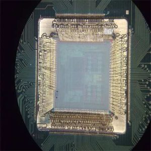
에 대한 연락하다 |
전화: +86 (0)755-8524-1496
이메일: info@alcantapcb.com

Cavity substrate 조작. High speed and high frequency material Cavity packaging substrate manufacturing. Advanced cavity(slot) production technique. we make the cavity PCBs from 4 레이어 30 레이어.

Do you want to know how Cavity Substrate in PCB (Printed Circuit Board) works? Cavity Substrate is a key technology that plays a vital role in PCB manufacturing. This article will deeply explore the definition, role and importance of Cavity Substrate in PCB 조작, helping readers fully understand the role and value of this key technology.

How is Cavity Substrate designed and manufactured?

Do you understand the design and manufacturing process of Cavity Substrate? As one of the key links in PCB manufacturing, Cavity Substrate plays a vital role in the performance and reliability of electronic devices. Let’s take a closer look at its design and manufacturing process.

가장 먼저, the design of Cavity Substrate is a critical step. Designers need to determine the Cavity’s size, 모양, and location based on the board’s requirements and the needs of the specific application. This step is usually accomplished with the help of CAD (computer-aided design) software. In CAD software, designers can accurately draw the structure of Cavity and make necessary adjustments and optimizations to ensure the performance and reliability of Cavity Substrate.

디자인이 완성되면, the next step is the manufacturing process. The first step in manufacturing Cavity Substrate is selecting the appropriate substrate material. Commonly used substrate materials include FR-4, metal substrates, 등., and the specific selection depends on factors such as the performance requirements of the circuit board and manufacturing costs. Choosing the right substrate material is critical to Cavity Substrate’s performance and cost.

다음, the manufacturer will process Cavity on the substrate according to the design requirements. This step usually involves mechanical or chemical processing to ensure that the size and shape of the Cavity meet the design requirements. After processing is complete, the manufacturer will surface treat Cavity to improve its corrosion resistance and thermal conductivity.

After completing the machining and surface treatment of Cavity, the next step is drilling and solder paste application. Drilling is for installing components and wires on Cavity Substrate, while solder paste coating is for soldering components. These steps require high-precision equipment and technology to ensure component installation quality and welding reliability.

마지막으로, the manufacturer will perform patch assembly and soldering, install the components onto the Cavity Substrate, and make solder connections. This step requires precise equipment and process control to ensure board performance and reliability.

요약하자면, the design and manufacturing of Cavity Substrate is a complex and critical process involving multiple links and technologies. Only by strictly controlling every detail during the design and manufacturing process can we ensure that the performance and reliability of Cavity Substrate meet the design requirements.

Cavity Substrate Manufacturing

What is the manufacturing process of Cavity Substrate?

When it comes to Cavity Substrate’s manufacturing process, there are numerous factors to consider. From material selection to final patch assembly and soldering, every step is critical and determines the quality and performance of the final product. Below we will introduce the manufacturing process of Cavity Substrate in detail.

첫 번째, let’s look at material selection. When manufacturing Cavity Substrate, choosing the right material is a crucial step. Common Cavity Substrate materials include FR4, aluminum substrates, ceramics, 등. These materials have different thermal conductivity, mechanical strength and electrical properties, so the selection of materials needs to be evaluated and selected based on actual needs.

Next is Cavity design and processing. Cavity refers to the grooves or holes cut out on the PCB board to accommodate specific components or parts. The design of Cavity needs to take into account the overall structure and circuit layout of the PCB to ensure that the connection and layout of Cavity and other components are consistent. Processing Cavity requires the use of precision cutting tools and equipment to ensure the Cavity’s size and shape meet the design requirements.

Then there is the hole drilling. Drilling holes on Cavity Substrate is for connecting and wiring electronic components. These holes need to be positioned and drilled accurately to ensure smooth subsequent welding and assembly work.

Next comes solder paste application. The purpose of applying solder paste on Cavity Substrate is to achieve soldering during the patch assembly process. Solder paste coating requires precise control of coating thickness and uniformity to ensure soldering quality and connection reliability.

Finally comes patch assembly and soldering. When performing patch assembly on Cavity Substrate, electronic components need to be placed precisely at designated locations and connected to the PCB board using soldering technology. The welding process requires temperature and time control to ensure welding quality and stability.

요약하자면, the manufacturing process of Cavity Substrate involves multiple key steps, including material selection, Cavity design and processing, hole drilling, solder paste coating, and patch assembly and welding. Each step requires precision operations and strict control to ensure the quality and performance of the final product meet expected requirements.

How to control the manufacturing cost of Cavity Substrate?

Are you concerned about how to control Cavity Substrate manufacturing costs? Cavity Substrate is an important part of PCB manufacturing, and its manufacturing cost directly affects the overall cost and product competitiveness. 그러므로, it is crucial to effectively control Cavity Substrate’s manufacturing costs. This section will explore the factors that affect the cost of Cavity Substrate and provide cost control strategies and methods.

Factors Affecting Cavity Substrate Cost

Material cost: The materials used in Cavity Substrate manufacturing directly affect the cost. Different types of substrates, metal layers, insulation layers and other materials have different prices, so choosing the right materials is crucial to cost control.

Production scale: Production scale is one of the important factors affecting costs. 일반적으로, large-scale production can reduce the manufacturing cost of a unit product, while small-scale production can increase the cost of a unit product.

Process and equipment: The use of advanced processes and equipment can improve production efficiency and reduce manufacturing costs. 하지만, the introduction of new processes and equipment also requires additional investment, and return on investment and cost-effectiveness need to be considered comprehensively.

Labor cost: Labor cost is an inevitable expense in the manufacturing process. Labor costs can be effectively controlled by optimizing production processes, improving employee efficiency, and reducing labor costs.

Quality Control: Low-quality products may result in additional costs such as rework and after-sales service. 그러므로, establishing a strict quality control system to ensure product quality can reduce additional costs and improve production efficiency.

Through the above strategies and methods, the manufacturing cost of Cavity Substrate can be effectively controlled and product competitiveness and market share can be improved. 그러므로, in the PCB manufacturing process, cost control is a crucial part and requires continuous attention and optimization.

What materials are used in Cavity Substrate?

When it comes to material selection for Cavity Substrate, there are several common options to consider. These materials have their own advantages and characteristics in different application scenarios, and have an important impact on the performance and cost of Cavity Substrate.

첫 번째, one of the most common Cavity Substrate materials is FR-4 (fiberglass reinforced epoxy). FR-4 has good mechanical strength and heat resistance and is suitable for most general electronic applications. Its cost is relatively low and it is the first choice of many manufacturers.

Another common option is a metal substrate, such as aluminum or copper. Metal substrates have excellent heat dissipation properties and are suitable for applications requiring high power and high temperature environments. 하지만, the cost of metal substrates is often higher and needs to be evaluated based on the specific application.

In some special application scenarios, high-performance materials such as polyimide (PI) or polyetheretherketone (몰래 엿보다) can also be considered. These materials have excellent high temperature resistance and chemical stability and are suitable for applications in high temperature, high frequency or extreme environments. 하지만, the cost of these high-performance materials is often higher, and there is a trade-off between performance and cost.

When selecting Cavity Substrate materials, factors such as performance, cost, and application environment need to be comprehensively considered. 예를 들어, in applications that require lower cost and average performance, FR-4 may be a more suitable choice, while in applications with high power, high temperature, or special environments, metal substrates or high-performance materials may need to be considered. 그러므로, for each specific project, careful evaluation and selection is required to ensure optimal performance and cost-effectiveness.

전반적인, Cavity Substrate’s material selection has a significant impact on its performance and cost. Understanding the characteristics and applicability of various materials, as well as comprehensive evaluation in specific projects, will help select the most appropriate materials to meet the needs of the project.

Who is making Cavity Substrate?

Do you know who manufactures Cavity Substrate in the PCB industry? Cavity Substrate manufacturers play a key role and are responsible for providing high-quality Cavity Substrate to meet the needs of their customers. There are several key factors to consider when choosing the right Cavity Substrate manufacturer.

첫 번째, the manufacturer’s experience and expertise are crucial. Choosing a manufacturer with extensive experience and a professional team ensures they understand your needs and provide products that meet standards. Such manufacturers can usually provide more reliable and stable products, helping you reduce production risks.

둘째, the manufacturer’s equipment and technical level are also important considerations. Advanced production equipment and technology can improve production efficiency and product quality, ensuring the stability and performance of Cavity Substrate. 그러므로, choosing a manufacturer with advanced equipment and technology can better meet your needs.

게다가, the manufacturer’s quality control system and certification status are also factors that need to be considered. Choosing manufacturers that have passed ISO and other relevant certifications can ensure that their product quality meets international standards and can meet customer quality requirements. 동시에, the manufacturer’s complete quality control system can also help promptly discover and solve potential problems to ensure stable and reliable product quality.

마지막으로, the manufacturer’s level of customer service is also a factor to consider. Choosing a manufacturer that can provide timely response, professional support and after-sales service can help you solve problems encountered in production and provide customized solutions to improve production efficiency and product quality.

When choosing a Cavity Substrate manufacturer, the above factors need to be taken into consideration. As a manufacturer with rich experience and a professional team, our company has advanced production equipment and technology, has passed ISO and other relevant certifications, and has a complete quality control system to provide high-quality Cavity Substrate and provide excellent customer service. Meet the various needs of customers. Choosing us as your Cavity Substrate manufacturing partner will be your wise choice.

What are the five characteristics of great customer service?

In the field of PCB manufacturing, providing excellent customer service is one of the key factors in ensuring customer satisfaction and business success. Below we’ll dive into the five characteristics of great customer service and their importance in the Cavity Substrate design and manufacturing process.

The first characteristic of great customer service is professional support. This includes having an experienced engineering team capable of providing customers with comprehensive technical advice and support. During the design and manufacturing process of Cavity Substrate, professional support can help customers solve various technical problems and ensure that the product meets design requirements and standards.

Prompt response and communication are the second hallmarks of great customer service. Customers expect timely responses and updates when they need them. During the Cavity Substrate manufacturing process, good communication ensures that customers are aware of project progress and can make adjustments or improvements when necessary.

The third feature is to provide customized solutions. Each customer’s needs may be different, so customized solutions can be provided to meet the customer’s specific needs and requirements. During the Cavity Substrate design and manufacturing process, customized solutions can help customers achieve their unique design goals and technical requirements.

Quality assurance is one of the key features of good customer service. Customers expect high quality and reliability from the products and services they purchase. During the Cavity Substrate manufacturing process, strict quality control and inspection procedures can ensure that products meet quality standards and reduce adverse effects caused by quality problems.

The last feature is the provision of effective after-sales support. Even after delivery is complete, the customer may require further support and services. During the Cavity Substrate manufacturing process, timely resolution of customer issues and provision of after-sales support can enhance customer trust and satisfaction with the company.

요약하자면, excellent customer service is one of the keys to the success of PCB manufacturing companies. By providing professional support, timely response and communication, customized solutions, quality assurance, and effective after-sales support, companies can win the trust and loyalty of their customers and achieve business success.

자주 묻는 질문

What are the advantages of using Cavity Substrates in PCBs?

Cavity Substrates offer several advantages, including improved thermal management, 전자기 간섭 감소, and enhanced mechanical stability. They also allow for greater design flexibility and integration of complex components, leading to higher performance and reliability in electronic devices.

How can one ensure the quality of Cavity Substrate manufacturing?

Ensuring quality in Cavity Substrate manufacturing requires strict adherence to industry standards and quality control measures throughout the production process. This includes thorough inspection of materials, precision machining techniques, and comprehensive testing of finished substrates to verify performance and reliability.

What role do Cavity Substrate manufacturers play in the PCB industry?

Cavity Substrate manufacturers play a critical role in the PCB industry by providing specialized expertise and capabilities for producing high-quality substrates tailored to specific application requirements. They collaborate closely with PCB designers and manufacturers to deliver innovative solutions and support technological advancements in electronic devices.

What trends are shaping the future of Cavity Substrate manufacturing?

Emerging trends in Cavity Substrate manufacturing include the development of advanced materials with enhanced thermal and electrical properties, the integration of additive manufacturing techniques for greater design flexibility, and the adoption of automated processes for increased efficiency and scalability. These trends are expected to drive further innovation and growth in the field of PCB manufacturing.

이전:

다음:

답장을 남겨주세요

이 사이트는 스팸을 줄이기 위해 Akismet을 사용합니다.. 댓글 데이터가 처리되는 방법 알아보기.