CO., LTD")
CSP substrate ya kifurushi Mtengenezaji. Utengenezaji wa substrate ya ufungaji wa vifaa vya kasi ya juu na masafa ya juu. Kampuni ya upakiaji ya hali ya juu.
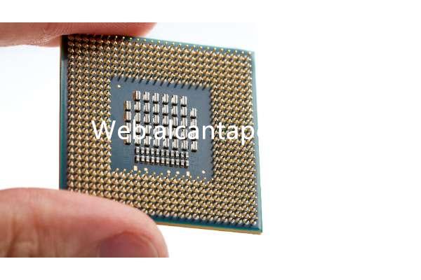
CSP Package Substrate, or Chip Scale Package Substrate, plays a vital role in Printed Circuit Boards (PCBs) by enabling seamless integration between semiconductor chips and circuit boards. In the current electronic packaging landscape, which prioritizes miniaturization and high efficiency, CSP Package Substrate stands out due to its unique design and functionalities.
One standout characteristic of CSP Package Substrate is its compact size. In comparison to traditional packaging methods, CSP Package Substrate boasts a more streamlined and smaller form, effectively utilizing space and enabling a compact PCB design. This downsized design contributes to smaller and lighter electronic devices, aligning with the growing demand from modern consumers for portability and convenience.
In addition to its size advantage, CSP Package Substrate offers outstanding performance characteristics. It maintains excellent electrical performance and ensures stable and reliable signal transmission. Wakati huo huo, CSP Package Substrate’s thermal management capabilities are also highly praised. Its design structure effectively dissipates heat and keeps the chip running within a suitable temperature range, thus improving the performance and life of electronic equipment.
The CSP Package Substrate plays a vital role in PCB engineering by enabling the smooth integration of semiconductor chips with circuit boards. It is crucial for supporting the miniaturization and performance enhancement of electronic devices. Serving as a major innovation in electronic packaging, CSP Package Substrate is set to stay at the forefront of PCB design and manufacturing, shaping the future direction of development in this field.
What types of CSP Package Substrate are there?
Katika Uhandisi wa kisasa wa PCB, CSP Package Substrate has become an indispensable choice for designers with its diverse types and wide range of applications. Learn more about the many types of CSP Package Substrates, from organic substrates to advanced HDI (Muunganisho wa Msongamano wa Juu) suluhisho, giving engineers a wealth of options. These types are explored in more detail below:
Sehemu ndogo za kikaboni, including materials like FR-4 and polyimide, are commonly used in CSP (Kifurushi cha kiwango cha chip) substrates for their strong mechanical and electrical properties, suitable for various electronic applications.
Sehemu ndogo za HDI, featuring elevated layer counts and minimized pitches, enable greater line density and intricate routing. They are particularly well-suited for compact spatial integration, making them optimal for applications such as smartphones and wearables.
Sehemu ndogo za polyimide, valued for their exceptional heat resistance and chemical stability, are employed in high-temperature settings like aerospace and automotive electronics. This guarantees stability and reliability even in extreme conditions.
Metal substrate CSP, employing materials like aluminum and copper, excels in thermal conductivity, making it suitable for applications requiring efficient heat dissipation, like LED lighting and power modules.
Sapphire substrate CSP, despite its higher cost, offers exceptional optical properties and wear resistance. Commonly used for packaging optoelectronic and high-power electronic devices, it provides unparalleled performance and reliability in specific applications.
Organic substrates are one of the most common types of CSP Package Substrate and are
The diverse types of CSP Package Substrate provide PCB engineers with a broad choice space, which can be flexibly selected according to specific design requirements and application scenarios. Ikiwa unafuata utendaji wa juu, high integration or excellent thermal management capabilities, you can find suitable solutions in different types of CSP Package Substrate.
What are the advantages of CSP Package Substrate?
CSP Package Substrate, as an innovative technology in the field of electronic design and manufacturing, has many advantages and provides a solid foundation for the development of more refined and efficient electronic devices.
CSP Package Substrate stands out in electrical performance due to its precise design and premium materials, ensuring a stable electrical connection and signal transmission. Katika maombi ya juu-frequency, it outperforms traditional packaging, minimizing signal distortion and interference while enhancing overall system performance.
Pili, CSP Package Substrate has excellent thermal management capabilities. Due to its smaller package size and higher density, CSP Package Substrate conducts and dissipates heat more efficiently. This helps reduce device temperatures, extend device life, na kuboresha utulivu wa mfumo, especially in high power density applications.
The CSP Package Substrate enhances space utilization through a compact design, enabling close integration of electronic components on the PCB. This results in efficient board space savings, offering greater flexibility in product design. Devices become thinner, nyepesi, na kubebeka zaidi, enhancing production efficiency and cost-effectiveness. Kwa muhtasari, the CSP Package Substrate delivers improved electrical performance, usimamizi bora wa joto, and optimized space utilization. These benefits not only bolster the performance and stability of electronic equipment but also fuel innovation and market competitiveness. Kadiri teknolojia inavyoendelea na matumizi yanavyopanuka, CSP Package Substrate is poised to play a pivotal role in future electronic design and manufacturing.
Why choose CSP Package Substrate?
In modern PCB projects, there are very valid reasons to choose CSP Package Substrate over traditional boards. CSP Package Substrate is increasingly popular in the field of electronic design due to its unique advantages. Here are some key factors:
CSP Package Substrate is known for its ultra-small size. They excel in space utilization compared to traditional boards. This compact shape makes them particularly suitable for high-density circuit layouts and can accommodate more functional modules in a limited space, thus providing the possibility for miniaturization and lightweighting of electronic equipment.
CSP Package Substrate goes far beyond traditional boards in terms of functionality. Kwa sababu ya muundo wake wa kompakt, CSP Package Substrate can accommodate more functional components such as integrated circuits, capacitors, na resistors. This enhanced functionality provides a solid foundation for improving the performance of electronic devices, allowing devices to achieve more complex and efficient operations.
CSP Package Substrate, incorporating cutting-edge manufacturing technology and advancements in materials science, proves highly compatible with state-of-the-art technologies. It effectively addresses the demands of contemporary PCB design, including high-speed data transmission, high-frequency signal processing, and advanced packaging techniques. The compact form factor, enhanced functionality, and compatibility with advanced technologies make CSP Package Substrate a superior choice over traditional boards. Its pivotal role in driving ongoing innovation within the electronics industry is undeniable. Kadiri teknolojia inavyoendelea, CSP Package Substrate is poised to remain a crucial contributor, fostering the innovation and evolution of electronic equipment.
How to make CSP Package Substrate?
The fabrication of CSP Package Substrate involves a meticulous and intricate manufacturing process comprising crucial steps to guarantee optimal performance and reliability. Katika utengenezaji wa substrate, state-of-the-art technologies, including electron beam lithography (EBL) and laser drilling, are employed to precisely create layers and interconnection vias. Uchaguzi wa nyenzo, such as FR-4 and polyimide, plays a pivotal role in enhancing durability and performance, with these options offering excellent mechanical properties, Upinzani wa joto la juu, na utulivu wa kemikali.
Chip assembly is a critical phase where chips are precisely integrated onto the substrate, ensuring high-density interconnections. Precision engineering techniques like micro-soldering and printed circuit board (PCB) routing are employed to achieve stable and reliable signal transmission. The use of cutting-edge technology and equipment, such as automated assembly lines and optical inspection systems, is paramount during chip assembly to enforce stringent quality control and meet performance standards.
Kwa muhtasari, the CSP Package Substrate manufacturing process demands the application of advanced technology, precise equipment, and adherence to strict quality control standards to ensure optimal performance and reliability in the final product.
What are the application areas of CSP Package Substrate?
The CSP Package Substrate finds extensive applications across diverse industries due to its versatility and adaptability. The compact dimensions and high-performance capabilities of CSP Package Substrate contribute to the development of sleek, portable designs in these devices, ensuring excellent performance and functionality.
Its high-density interconnection and superior thermal management meet stringent stability, kuegemea, and performance requirements in automotive applications.
The aerospace sector also benefits from CSP Package Substrate in flight control systems, vifaa vya mawasiliano, na mifumo ya urambazaji. Its lightweight and integrated characteristics contribute to improved performance and efficiency in aerospace electronics.
Within the medical device manufacturing realm, CSP Package Substrate is prevalent in various diagnostic, matibabu, na mifumo ya ufuatiliaji wa mgonjwa. Its high integration and reliability meet stringent stability, accuracy, and reliability requirements, providing crucial support to the medical industry.
How to obtain CSP Package Substrate?
We are a trusted manufacturer dedicated to delivering top-notch CSP Package Substrate for your projects. Our commitment lies in ensuring superior product quality, kuegemea, na uvumbuzi. Employing high-standard quality control processes, we meticulously oversee material selection and production to guarantee industry-leading levels of quality.
Our CSP Package Substrate undergoes rigorous reliability testing to ensure stable performance in various environmental conditions, including extremes of temperature and high-frequency operations. As pioneers in the industry, we regularly introduce cutting-edge technologies and processes, dedicating resources to ongoing research and development to continually improve the product’s performance and functionality.
Our customer service team is ready to provide support and consultation, tailoring solutions to meet your project requirements. Partnering with us ensures access to high-quality, ya kuaminika, and innovative CSP Package Substrate, injecting new energy and competitiveness into your projects. We eagerly anticipate collaborating with you to advance the field of electronic engineering.
What is the quote for CSP Package Substrate?
Selecting a CSP Package Substrate involves prioritizing price, yet partnering with a reliable manufacturer is paramount for project success and dependability. To ensure a high-quality substrate, focus on reputable manufacturers with extensive industry experience, adhering to stringent quality standards and embracing innovation.
Before finalizing a manufacturer, understand their quality control protocols, encompassing production checks, material and technology utilization, and testing methods for product performance and reliability. A manufacturer with a dependable supply chain is essential, ensuring a stable flow of raw materials and timely order deliveries to prevent production delays.
Prior to making a decision, reach out to the manufacturer’s existing clients to gather insights into their experiences and feedback. This step aids in assessing the manufacturer’s credibility and product quality. Establishing long-term relationships with manufacturers fosters trust, enabling effective collaboration to address challenges and drive innovation.
While price is a significant factor, it should not compromise quality and reliability when selecting a CSP Package Substrate manufacturer. Partnering with a trustworthy manufacturer guarantees not only top-notch products but also technical support and ongoing innovation, establishing a solid foundation for project success.
Maswali yanayoulizwa mara kwa mara
What are CSP Package Substrates?
CSP Package Substrates are foundational components in PCB engineering, facilitating the integration of semiconductor chips onto circuit boards. They represent advanced packaging technology characterized by miniaturization and efficiency.
What types of CSP Package Substrates are available?
CSP Package Substrates come in various types, including organic substrates and HDI (Uunganisho wa kiwango cha juu) suluhisho. Each type offers unique features catering to different design requirements.
What are the advantages of CSP Package Substrates?
CSP Package Substrates offer several advantages, such as enhanced electrical performance, usimamizi bora wa joto, and optimized space utilization. These benefits contribute to the development of sleeker and more efficient electronic devices.
Why choose CSP Package Substrates over other board types?
CSP Package Substrates excel in compactness, utendakazi, na utangamano na teknolojia za hali ya juu, making them a preferred choice for modern PCB designs seeking optimal performance within limited space constraints.
How are CSP Package Substrates manufactured?
The manufacturing process involves precision engineering techniques for substrate fabrication and chip assembly. Advanced materials and technologies are utilized to ensure high-quality and reliable performance.
Are CSP Package Substrates compatible with specific electronic devices?
CSP Package Substrates offer flexibility and customization options to meet the requirements of different electronic devices. They can be tailored to specific applications, ensuring compatibility and optimal performance.
What is CSP Package Substrate?
CSP Package Substrate is a pivotal component in PCBs, serving as a foundational bridge for integrating semiconductor chips onto the board. It embodies miniaturization and efficiency, enabling compact yet high-performance electronic packaging.
What types of CSP Package Substrates are available?
CSP Package Substrates come in various types, including organic substrates and advanced HDI (Uunganisho wa kiwango cha juu) suluhisho. Each type caters to specific design requirements, offering engineers a range of options for diverse projects.
What advantages do CSP Package Substrates offer?
CSP Package Substrates boast advantages such as enhanced electrical performance, usimamizi bora wa joto, and optimized space utilization. These features collectively contribute to the development of sleeker, vifaa vya elektroniki vya ufanisi zaidi.