CO., LTD")
FCCSP (Flip Chip Scale Package) mtengenezaji wa substrates, Ultra-Multilayer FCCSP (Chip ya Flip Kifurushi cha kiwango cha chip) substrates ni masuluhisho ya hali ya juu ya vifungashio yaliyoundwa kusaidia ugumu unaoongezeka na mahitaji ya utendaji wa vifaa vya kisasa vya kielektroniki. Sehemu ndogo hizi zina tabaka nyingi za mzunguko, kuwezesha viunganishi vya juu-wiani na usimamizi bora wa joto. Vipande vidogo vya Ultra-Multilayer FCCSP ni muhimu katika programu ambapo uboreshaji mdogo, Utendaji wa hali ya juu, na kuaminika ni muhimu, kama vile kwenye simu mahiri, Kompyuta ya utendaji wa juu, na mawasiliano ya simu.
Je! Sehemu ndogo ya Ultra-Multilayer FCCSP ni nini?
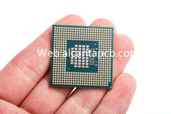
Kipande kidogo cha Ultra-Multilayer FCCSP ni aina ya sehemu ndogo ya kifurushi cha semiconductor iliyoundwa ili kusaidia kuunganisha chip na safu nyingi za sakiti.. Teknolojia ya FCCSP inahusisha kupachika semiconductor kufa uso chini kwenye substrate, kuruhusu miunganisho ya umeme ya moja kwa moja kati ya divai na sehemu ndogo kupitia matuta ya solder. Njia hii ya ufungaji hupunguza saizi ya kifurushi na huongeza utendaji wa umeme kwa kupunguza urefu wa viunganisho.
The “tabaka nyingi zaidi” kipengele kinarejelea matumizi ya tabaka nyingi za saketi ndani ya substrate. Tabaka hizi huwezesha uelekezaji wa juu-wiani wa ishara na nguvu, ambayo ni muhimu kwa kusaidia kazi ngumu na ya kasi ya vifaa vya kisasa vya semiconductor. Sehemu ndogo za Ultra-Multilayer FCCSP hutoa utimilifu wa mawimbi ulioboreshwa, usambazaji wa nguvu wenye ufanisi, na usimamizi wa mafuta ulioboreshwa, kuwafanya kuwa bora kwa programu za utendaji wa juu.
Mwongozo wa Marejeleo wa Usanifu wa Kitengo kidogo cha Ultra-Multilayer FCCSP
Kubuni substrates za Ultra-Multilayer FCCSP huhusisha mambo kadhaa muhimu ili kuhakikisha utendakazi bora na kutegemewa.. Sehemu zifuatazo zinatoa muhtasari wa vipengele muhimu vinavyohusika katika uundaji na matumizi ya substrates hizi.
Nyenzo zinazotumika katika vijenzi vidogo vya Ultra-Multilayer FCCSP huchaguliwa kwa ubora wake wa juu wa umeme, mafuta, na mali ya mitambo:
Nyenzo za Dielectric za Utendaji wa Juu: Vifaa vya juu vya dielectric, kama vile poliimidi na polima kioevu kioo, hutumika kutoa insulation bora ya umeme na kusaidia upitishaji wa ishara ya masafa ya juu.
Shaba: Tabaka za shaba nyembamba sana hutumiwa kwa athari za conductive, kutoa upitishaji bora wa umeme na kuruhusu muundo wa laini-fine muhimu kwa viunganishi vya msongamano wa juu.
Mask ya Solder: Kinyago cha usahihi wa hali ya juu kinatumika kulinda sakiti ya msingi na kuzuia kuunganishwa kwa solder wakati wa kusanyiko.. Mask ya solder lazima ihimili joto la juu la kusambaza tena na michakato mingine ya mkusanyiko.
Adhesives: Adhesives ya juu hutumiwa kuunganisha tabaka pamoja, kuhakikisha utulivu wa mitambo na kupunguza upotevu wa ishara.
Mambo kadhaa muhimu yanapaswa kushughulikiwa wakati wa awamu ya kubuni:
Udhibiti wa Impedans: Udhibiti sahihi wa impedance ni muhimu kwa kudumisha uadilifu wa ishara, hasa katika masafa ya juu. Hii inahusisha uundaji wa makini wa athari za ishara na matumizi ya vifaa vya kudhibiti impedance.
Usimamizi wa mafuta: Udhibiti mzuri wa mafuta ni muhimu kwa programu zenye utendaji wa juu. Muundo lazima ujumuishe vias ya joto, Joto huzama, au mbinu nyingine za kusambaza joto linalotokana na vipengele vya nguvu ya juu.
Utulivu wa Mitambo: Sehemu ndogo lazima itoe usaidizi thabiti wa kiufundi ili kuhimili baiskeli ya joto na mikazo ya mitambo wakati wa operesheni..
Kuegemea: Kuegemea kwa muda mrefu kunahakikishwa kupitia matumizi ya vifaa vya hali ya juu na michakato sahihi ya utengenezaji, kuzuia masuala kama vile delamination na warping.
Ni Nyenzo Gani Zinazotumika katika Vidogo Vidogo vya Ultra-Multilayer FCCSP?
Nyenzo zinazotumiwa katika vijenzi vidogo vya Ultra-Multilayer FCCSP huchaguliwa kwa ajili ya sifa zake za ziada ili kuimarisha utendakazi wa jumla wa substrate.:
Nyenzo za Dielectric za Utendaji wa Juu: Vifaa vya juu vya dielectric hutoa insulation ya umeme na kusaidia maambukizi ya ishara ya juu-frequency.
Shaba: Shaba ya usafi wa juu hutumiwa kwa tabaka za conductive, kutoa upitishaji bora wa umeme na kuwezesha muundo wa laini laini.
Mask ya Solder: Nyembamba, kinyago cha usahihi wa hali ya juu hulinda sakiti ya msingi na huzuia uwekaji madaraja wakati wa kuunganisha, kuhimili joto la juu la soldering reflow.
Adhesives ya juu: Adhesives maalumu huunganisha tabaka pamoja, kutoa utulivu wa mitambo na kupunguza kupoteza kwa ishara.
Ukubwa Gani ni Vidogo vya Ultra-Multilayer FCCSP?
Ukubwa wa substrates za Ultra-Multilayer FCCSP hutofautiana kulingana na programu na mahitaji mahususi ya muundo:
Unene: Unene wa jumla wa substrates za Ultra-Multilayer FCCSP zinaweza kuanzia mikromita mia chache hadi zaidi ya milimita., kulingana na idadi ya tabaka na mahitaji ya maombi.
Vipimo: Urefu na upana wa substrates hutambuliwa na ukubwa wa vipengele na mpangilio wa mfumo. Wanaweza kuanzia vipengele vidogo vya umbo la vifaa vya kompakt hadi substrates kubwa kwa mifumo changamano zaidi ya kielektroniki.
Mchakato wa Utengenezaji wa Vidogo vya Ultra-Multilayer FCCSP
Mchakato wa utengenezaji wa vijembe vya Ultra-Multilayer FCCSP vinahusisha hatua kadhaa sahihi na zinazodhibitiwa ili kuhakikisha ubora wa juu na utendakazi.:
Vifaa vya msingi vya ubora wa juu, kama vile laminates za shaba na vifaa vya juu vya dielectric, huchaguliwa na kutayarishwa kwa usindikaji. Nyenzo husafishwa na kutibiwa ili kuondoa uchafu wowote na kuhakikisha uso laini.
Nyenzo ya dielectric hutumiwa kwenye substrate katika tabaka nyingi, huku kila safu ikichorwa na kuponywa ili kuunda mifumo ya saketi inayotakiwa. Utaratibu huu unarudiwa ili kuunda idadi inayotakiwa ya tabaka, kuhakikisha viunganishi vya juu-wiani na utendaji bora wa umeme.
Microvias na kupitia-mashimo hupigwa kwenye substrate ili kuunda uhusiano wa umeme kati ya tabaka. Vias hivi basi huwekwa kwa shaba ili kuhakikisha upitishaji wa umeme unaotegemewa na usaidizi thabiti wa mitambo.
Sehemu ya sehemu ndogo imekamilishwa kwa kinyago cha usahihi wa hali ya juu ili kulinda saketi ya msingi na kutoa uso laini wa kupachika sehemu.. Hatua hii pia inajumuisha matumizi ya faini za uso, kama vile enig (Electroless nickel kuzamisha dhahabu) au OSP (Uhifadhi wa Kikaboni), ili kuongeza uwezo wa kuuzwa na kutu.
Baada ya kutengeneza, substrates hukusanywa na vipengele vya elektroniki. Upimaji mkali unafanywa ili kuhakikisha kwamba substrates zinakidhi vipimo vyote vya muundo na mahitaji ya utendaji. Hii ni pamoja na kupima umeme, Baiskeli ya mafuta, na upimaji wa mkazo wa kimitambo ili kuthibitisha kutegemewa na uimara wa substrates.
Eneo la Maombi la Vidogo vya Ultra-Multilayer FCCSP
Sehemu ndogo za FCCSP za Ultra-Multilayer hutumiwa katika anuwai ya programu za kielektroniki za utendaji wa juu:
Katika vifaa vya elektroniki vya watumiaji, Vipande vidogo vya Ultra-Multilayer FCCSP vinaauni vifaa vyenye utendakazi wa juu na kompakt kama vile simu mahiri, vidonge, na teknolojia inayoweza kuvaliwa. Substrates hutoa utendaji muhimu wa umeme na joto ili kuhakikisha uendeshaji wa kuaminika wa vifaa hivi.
Katika vifaa vya matibabu, Vipande vidogo vya Ultra-Multilayer FCCSP vinasaidia usindikaji wa mawimbi ya masafa ya juu na uendeshaji unaotegemewa katika vifaa mbalimbali vya uchunguzi na matibabu.. Substrates hizi huhakikisha upitishaji wa ishara sahihi na sahihi, kuzifanya kuwa bora kwa matumizi katika mifumo ya picha, vifaa vya ufuatiliaji, na vyombo vya upasuaji.
Katika Maombi ya Magari, Vipande vidogo vya Ultra-Multilayer FCCSP vinatumika katika mifumo mbalimbali ya kielektroniki, ikiwa ni pamoja na infotainment, urambazaji, na mifumo ya juu ya usaidizi wa madereva (Adas). Substrates hizi hutoa uaminifu wa juu na utendaji, kuwezesha utendakazi wa hali ya juu na uendeshaji bora katika mazingira ya magari.
Katika anga na maombi ya ulinzi, Sehemu ndogo za FCCSP za Ultra-Multilayer hutoa utendakazi dhabiti katika mazingira magumu na chini ya hali mbaya zaidi. Substrates hizi hutumiwa katika mifumo mbalimbali ya anga na ulinzi, kama vile rada, mawasiliano, na mifumo ya urambazaji, kuhakikisha uendeshaji wa kuaminika na uimara wa muda mrefu.
Katika automatisering ya viwanda, Vipande vidogo vya Ultra-Multilayer FCCSP vinatumika katika mifumo mbalimbali ya udhibiti na otomatiki. Substrates hizi hutoa uaminifu wa juu na utendaji, kuwezesha utendaji wa hali ya juu na uendeshaji bora katika mazingira ya viwanda.
Je, ni Manufaa ya Vidogo vya Ultra-Multilayer FCCSP?
Vipande vidogo vya Ultra-Multilayer FCCSP vinatoa faida kadhaa zinazozifanya ziwe muhimu katika utendakazi wa juu wa programu za kielektroniki.:
Utendaji wa Juu: Sehemu ndogo za Ultra-Multilayer FCCSP hutoa usindikaji wa mawimbi ya kasi ya juu na uadilifu bora wa mawimbi, kuwafanya kuwa bora kwa vifaa na mifumo ya hali ya juu ya elektroniki.
Miniaturization: Substrates hizi huwezesha ujumuishaji wa saketi changamano katika kipengele cha umbo la kompakt, kusaidia mwelekeo kuelekea vifaa vidogo na vyenye nguvu zaidi vya kielektroniki.
Usimamizi wa mafuta: Substrates hizi hutoa usimamizi bora wa joto, kwa ufanisi kusambaza joto linalotokana na vipengele vya juu-nguvu na kuhakikisha uendeshaji wa kuaminika.
Kupunguza Warpage: Matumizi ya nyenzo za hali ya juu na michakato sahihi ya utengenezaji hupunguza hatari ya vita, kuboresha utulivu wa mitambo na uaminifu wa substrate.
Kuegemea: Sehemu ndogo za FCCSP za Ultra-Multilayer hutoa usaidizi thabiti wa kiufundi, Usimamizi mzuri wa mafuta, na kuegemea kwa muda mrefu, kuhakikisha uendeshaji thabiti wa vifaa vya elektroniki.
Uwezo mwingi: Vipande vidogo vya Ultra-Multilayer FCCSP vinaweza kutumika katika matumizi mbalimbali, kutoka kwa vifaa vya kielektroniki vya watumiaji na vifaa vya matibabu hadi magari na anga, kutoa utendaji wa hali ya juu na kuegemea katika mazingira yanayohitaji.
Maswali
Je, ni mambo gani ya kuzingatia katika kubuni kitengo kidogo cha Ultra-Multilayer FCCSP?
Mambo muhimu ya kuzingatia ni pamoja na mali ya nyenzo, safu-up, udhibiti wa impedance, Usimamizi wa mafuta, na utulivu wa mitambo. Ubunifu unapaswa kuhakikisha utendaji bora wa umeme, ufanisi wa uharibifu wa joto, na kuegemea kwa muda mrefu.
Jinsi sehemu ndogo za Ultra-Multilayer FCCSP hutofautiana na substrates za jadi za FCCSP?
Vipande vidogo vya FCCSP vya Ultra-Multilayer vina tabaka nyingi za sakiti, kuwezesha uelekezaji wa msongamano wa juu na utendakazi ulioimarishwa wa umeme ikilinganishwa na substrates za jadi za FCCSP, ambayo inaweza kuwa na tabaka chache na viunganishi vya chini vya msongamano.
Je, ni mchakato gani wa kawaida wa utengenezaji wa substrates za Ultra-Multilayer FCCSP?
Mchakato unahusisha maandalizi ya nyenzo, uundaji wa safu, kuchimba visima na plating, kumaliza uso, na mkusanyiko na upimaji. Kila hatua inadhibitiwa kwa uangalifu ili kuhakikisha ubora wa juu na utendaji.