CO., LTD")
Mtengenezaji wa Vifurushi vya Kifurushi cha GPU.Kama GPU inayoongoza substrates za kifurushi mtengenezaji, Sisi utaalam katika kutoa utendaji wa juu, suluhisho za kuaminika kwa vitengo vya usindikaji wa picha za hali ya juu. Vifaa vyetu vya hali ya juu na uhandisi wa ubunifu huhakikisha ubora wa hali ya juu na usahihi katika kila bidhaa. Tunakidhi mahitaji ya lazima ya michezo ya kubahatisha, Ai, na viwanda vya kituo cha data, kutoa substrates zinazoboresha usimamizi wa joto, Uadilifu wa ishara, na utendaji kwa ujumla. Tuamini kwa teknolojia ya kisasa ya upakiaji ya GPU ambayo huleta mustakabali wa kompyuta.
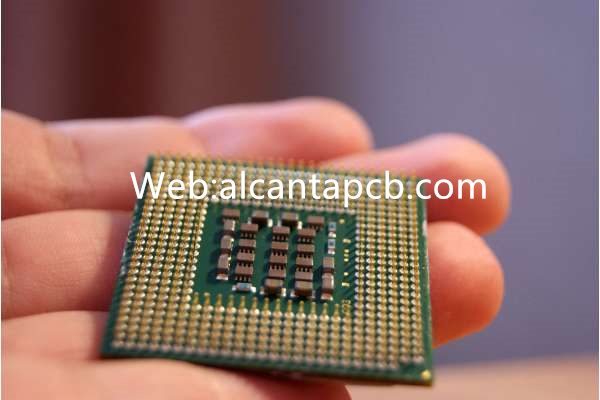
GPU (Kitengo cha Uchakataji wa Michoro) substrates za kifurushi ni sehemu muhimu katika kompyuta ya kisasa, kutoa jukwaa la msingi la kupachika na kuunganisha vipengele mbalimbali vya kielektroniki vya GPU. Sehemu ndogo hizi zimeundwa kusaidia ujumuishaji wa msongamano wa juu na usimamizi bora wa joto unaohitajika kwa usindikaji wa utendaji wa juu wa michoro.. Kadiri GPU zinavyozidi kuwa muhimu katika anuwai ya programu, kutoka kwa michezo ya kubahatisha na michoro ya kitaalamu hadi akili bandia na kompyuta ya kisayansi, jukumu la sehemu ndogo za kifurushi cha GPU ni muhimu zaidi kuliko hapo awali. Makala hii inachunguza sifa, muundo, vifaa, Mchakato wa utengenezaji, Maombi, na faida za substrates za kifurushi cha GPU.
Sehemu ndogo ya Kifurushi cha GPU ni nini?
Sehemu ndogo ya kifurushi cha GPU ni aina ya nyenzo za msingi zinazotumiwa kukusanya na kuunganisha vipengele vya kitengo cha usindikaji wa michoro.. Inatumika kama mpatanishi kati ya chip ya silicon na bodi ya mzunguko iliyochapishwa (PCB), kutoa msaada wa mitambo na kuunganishwa kwa umeme. Sehemu ndogo za kifurushi cha GPU zimeundwa ili kushughulikia nyaya zenye msongamano mkubwa na miunganisho changamano inayohitajika na GPU za kisasa..
Sehemu ndogo za kifurushi cha GPU kawaida hutengenezwa kutoka kwa nyenzo za hali ya juu ambazo hutoa insulation bora ya umeme, Uboreshaji wa mafuta, na utulivu wa mitambo. Ni muhimu kwa ufungaji wa GPU, kuhakikisha kwamba vipengele vya semiconductor dhaifu vinalindwa na vinaweza kufanya kazi kwa ufanisi chini ya hali ya juu ya utendaji..
Muundo wa Vidogo vya Kifurushi cha GPU
Muundo wa substrates za kifurushi cha GPU ni ngumu na yenye safu nyingi, iliyoundwa ili kukidhi mahitaji yanayohitajika ya uchakataji wa utendakazi wa hali ya juu. Mambo muhimu ya kimuundo ni pamoja na:
Safu ya msingi huunda muundo wa msingi wa substrate, kutoa utulivu wa mitambo na rigidity. Kawaida hutengenezwa kutoka kwa nyenzo kama vile resin ya epoxy iliyoimarishwa kwa glasi au keramik.
Tabaka hizi zinaongezwa juu ya safu ya msingi ili kuongeza wiani wa wiring na kusaidia mifumo tata ya mzunguko. Tabaka za kujenga-up zinajengwa kwa kutumia vifaa vya juu vya dielectric ili kuhakikisha utendaji bora wa umeme.
Tabaka za conductive, kawaida hutengenezwa kwa shaba, kuunda athari za mzunguko zinazounganisha vipengele mbalimbali kwenye substrate. Safu hizi zimechorwa kwa kutumia michakato ya picha ili kuunda wiring sahihi na wa juu.
Via ni viunganishi vya wima vinavyounganisha tabaka tofauti za substrate. Wao huundwa kwa kutumia mbinu za juu za kuchimba visima, kama vile kuchimba laser, ili kuhakikisha usahihi wa juu na kuegemea.
Uso unamalizia, kama vile Dhahabu ya Kuzamishwa ya Nikeli Isiyo na Electroless (KUBALI) au Kihifadhi cha Kutengemaa Kikaboni (OSP), hutumika kwa usafi wa mawasiliano ili kuboresha uuzwaji na kulinda dhidi ya oxidation.
Mask ya solder hutumiwa kulinda athari za conductive kutokana na uharibifu wa mazingira na kuzuia madaraja ya solder wakati wa kusanyiko.
Nyenzo Zinazotumika katika Kifurushi Kidogo cha GPUes
Uchaguzi wa nyenzo kwa substrates za kifurushi cha GPU ni muhimu kwa utendaji wao na uaminifu. Nyenzo muhimu ni pamoja na:
Resini za epoxy, mara nyingi huimarishwa na fiberglass, hutumiwa kwa kawaida kwa tabaka za msingi na za kujenga. Nyenzo hizi hutoa nguvu bora za mitambo na utulivu wa joto.
Keramik ya utendaji wa juu, kama vile alumina na aluminium nitride, hutumiwa katika sehemu ndogo za kifurushi cha GPU ili kutoa upitishaji wa hali ya juu wa mafuta na insulation ya umeme.
Copper hutumiwa sana kwa tabaka za conductive kutokana na conductivity bora ya umeme. Foili nyembamba za shaba hutiwa laminated kwenye substrate na kupangwa ili kuunda athari za mzunguko.
Nyenzo za hali ya juu za dielectric zilizo na viwango vya chini vya dielectric na tanjenti za upotezaji wa chini hutumiwa kuhakikisha upunguzaji mdogo wa mawimbi na utendaji wa masafa ya juu..
ENIG na OSP ni vifaa vya kumalizia uso vinavyotumika kwa kawaida ili kuboresha uuzwaji na kulinda pedi za mguso dhidi ya uoksidishaji na kutu..
Mchakato wa Utengenezaji wa Vifungu vidogo vya Kifurushi cha GPU
Mchakato wa utengenezaji wa substrates za kifurushi cha GPU unahusisha hatua kadhaa sahihi na zinazodhibitiwa ili kuhakikisha ubora wa juu na utendakazi. Hatua muhimu ni pamoja na:
Malighafi yenye ubora wa juu, ikiwa ni pamoja na resini za epoxy, foils za shaba, na filamu za dielectric, yanatayarishwa na kukaguliwa ili kuhakikisha kuwa yanakidhi vigezo vinavyohitajika.
Safu ya msingi na tabaka za kujenga zimeunganishwa pamoja kwa kutumia joto na shinikizo ili kuunda substrate iliyounganishwa. Hatua hii inahusisha upatanishi sahihi na udhibiti ili kuhakikisha tabaka zimeunganishwa ipasavyo.
Vias na kupitia-mashimo huchimbwa kwenye substrate ili kuunda miunganisho ya umeme kati ya tabaka. Shimo hizi huwekwa na shaba ili kuanzisha njia za kusisimua.
Mifumo ya mzunguko huundwa kwa kutumia michakato ya picha. Hii inahusisha kutumia filamu ya picha (Mpiga picha) kwa uso wa shaba, kuionyesha kwa ultraviolet (UV) mwanga kupitia mask, na kuendeleza maeneo yaliyo wazi ili kufichua mifumo ya saketi inayotakiwa. Kisha substrate imewekwa ili kuondoa shaba isiyohitajika, kuacha nyuma athari za mzunguko.
Mask ya solder hutumiwa kwenye substrate ili kulinda mzunguko na kuzuia madaraja ya solder wakati wa mkusanyiko. Mask ya solder kawaida hutumiwa kwa uchapishaji wa skrini au mbinu za upigaji picha na kisha kutibiwa ili kuifanya iwe ngumu..
Finishio za uso huwekwa kwenye pedi za mguso ili kuongeza uwezakano wa kuuzwa na kulinda dhidi ya uoksidishaji. Mbinu kama ENIG au OSP hutumiwa kuhakikisha viungo vya kuaminika vya solder na uimara wa muda mrefu..
Sehemu ndogo za mwisho hukaguliwa na kufanyiwa majaribio ya kina ili kuhakikisha kwamba zinaafiki viwango vyote vya utendakazi na kutegemewa. Upimaji wa umeme, ukaguzi wa kuona, na ukaguzi wa otomatiki wa macho (Aoi) hutumika kutambua kasoro au kasoro zozote.
Maeneo ya Utumizi ya Vifungu vidogo vya Kifurushi cha GPU
Sehemu ndogo za kifurushi cha GPU hutumiwa katika anuwai ya programu za kielektroniki katika tasnia mbalimbali. Maeneo muhimu ya maombi ni pamoja na:
GPU ni muhimu kwa kutoa michoro ya ubora wa juu katika kiweko cha michezo ya kubahatisha, Kompyuta, na mifumo ya ukweli halisi. Sehemu ndogo za kifurushi cha GPU hutoa utendaji unaohitajika na kutegemewa kwa programu hizi zinazohitajika.
Katika tasnia kama vile uhuishaji, utengenezaji wa filamu, na muundo wa picha, GPU hutumiwa kutoa michoro changamano na athari za kuona. Sehemu ndogo za kifurushi cha GPU zinaauni mahitaji ya utendaji wa juu wa programu hizi za kitaaluma.
GPU zinazidi kutumika kwa AI na kazi za kujifunza mashine kutokana na uwezo wao wa kuchakata sambamba. Sehemu ndogo za kifurushi cha GPU huwezesha ujumuishaji wa msongamano wa juu na usimamizi bora wa mafuta unaohitajika kwa mzigo wa kazi wa AI..
Katika utafiti wa kisayansi na masimulizi, GPU huharakisha hesabu changamano na uchanganuzi wa data. Sehemu ndogo za kifurushi cha GPU huhakikisha utendakazi unaotegemewa katika programu hizi za kiwango cha juu.
GPU hutumiwa katika mifumo ya juu ya usaidizi wa madereva (Adas) na teknolojia za kuendesha gari zinazojitegemea. Sehemu ndogo za kifurushi cha GPU hutoa utendaji unaohitajika na uimara wa programu hizi za magari.
Manufaa ya Vidogo vya Kifurushi cha GPU
Sehemu ndogo za kifurushi cha GPU hutoa faida kadhaa ambazo zinawafanya kuwa wa lazima kwa programu za kisasa za kompyuta. Faida hizi ni pamoja na:
Sehemu ndogo za kifurushi cha GPU zinaunga mkono ujumuishaji wa msongamano wa juu wa vipengee vya kielektroniki, kuwezesha ujumuishaji wa utendakazi changamano na kuboresha utendaji kwa ujumla.
Nyenzo za hali ya juu na michakato mahususi ya utengenezaji inayotumika katika vifurushi vidogo vya GPU huhakikisha upotezaji mdogo wa mawimbi na kuingiliwa, kusababisha utendaji bora wa umeme.
Sehemu ndogo za kifurushi cha GPU zimeundwa ili kusambaza joto kwa ufanisi, kuzuia joto kupita kiasi na kuhakikisha uendeshaji wa kuaminika wa vipengele vya GPU.
Ujenzi dhabiti na nyenzo za ubora wa juu zinazotumiwa katika sehemu ndogo za kifurushi cha GPU huhakikisha utendakazi unaotegemewa katika mazingira yanayohitajika. Sehemu ndogo hizi zimeundwa kustahimili baiskeli ya joto, Mkazo wa mitambo, na hali ngumu.
Maswali
Ni nini kinachofanya substrates za kifurushi cha GPU kufaa kwa programu za kompyuta zenye utendaji wa juu?
Sehemu ndogo za kifurushi cha GPU zinafaa kwa programu za kompyuta zenye utendakazi wa hali ya juu kwa sababu ya muunganisho wao wa msongamano wa juu., kuimarishwa kwa utendaji wa umeme, Usimamizi mzuri wa mafuta, na mali imara za mitambo. Tabia hizi huwezesha uendeshaji wa kuaminika na ufanisi katika mazingira ya kudai.
Je, substrates za kifurushi cha GPU zinaweza kutumika katika mazingira yenye halijoto ya juu?
Ndio, Sehemu ndogo za kifurushi cha GPU zinafaa sana kwa mazingira ya halijoto ya juu. Uwezo wao bora wa usimamizi wa mafuta na ujenzi thabiti huhakikisha utendaji wa kuaminika chini ya dhiki ya joto, kuzifanya kuwa bora kwa programu kama vile michezo ya kubahatisha na michoro ya kitaalamu.
Je, sehemu ndogo za kifurushi cha GPU huhakikisha vipi usimamizi mzuri wa mafuta?
Sehemu ndogo za kifurushi cha GPU huhakikisha usimamizi mzuri wa mafuta kupitia utumiaji wa nyenzo za hali ya juu zilizo na upitishaji wa hali ya juu wa mafuta na miundo bora ya mafuta.. Vipengele hivi hurahisisha utaftaji wa joto kutoka kwa vijenzi vya GPU hadi substrate, kuzuia overheating na kuhakikisha uendeshaji wa kuaminika.
Ni tasnia gani zinazonufaika zaidi kwa kutumia substrates za kifurushi cha GPU?
Sekta zinazonufaika zaidi kutokana na kutumia vifurushi vidogo vya GPU ni pamoja na michezo ya kubahatisha na burudani, graphics za kitaaluma, akili ya bandia, kompyuta ya kisayansi, na magari. Sekta hizi zinahitaji ushirikiano wa juu-wiani, kuimarishwa kwa utendaji wa umeme, na usimamizi mzuri wa mafuta, ambayo sehemu ndogo za kifurushi cha GPU hutoa.