CO., LTD")
Sura ya risasi ya mtengenezaji wa kifurushi cha QFN, Sura ya chuma ya QFN uzalishaji, Tumefanya matibabu ya uso wa chuma wa QFN na upangaji wa fedha au labda au upangaji wa au, kuhusu unene wa fedha na au, Tutaweka unene kulingana na hitaji lako.
Katika ulimwengu wa ufungaji wa semiconductor, sura inayoongoza ina jukumu muhimu, hasa katika QFN (Quad Flat No-LEAD) vifurushi. Kwa kuongezeka kwa mahitaji ya uboreshaji mdogo na utendakazi ulioimarishwa katika vifaa vya kielektroniki, Vifurushi vya QFN vimekuwa chaguo maarufu kwa sababu ya saizi yao ngumu, utendaji wa joto, na ufanisi wa gharama. Sura ya kuongoza ni sehemu muhimu katika mchakato huu wa ufungaji, kutoa msaada wa mitambo na uunganisho wa umeme. Makala haya yanaangazia umuhimu wa fremu ya kuongoza katika vifurushi vya QFN, kuonyesha muundo wake, faida, na mchakato wa utengenezaji.
Je! Muundo wa Kuongoza ni nini?
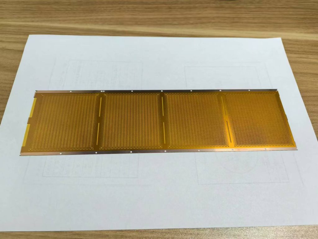
Sura ya risasi ni muundo wa chuma, kawaida hutengenezwa kutoka kwa shaba au aloi ya shaba, ambayo ni uti wa mgongo wa IC nyingi (Mzunguko Uliounganishwa) vifurushi. Katika muktadha wa ufungaji wa QFN, sura ya risasi hufanya kazi kadhaa muhimu. Inatoa msingi wa kuweka semiconductor kufa, huunganisha kufa na mizunguko ya nje, na husaidia kudhibiti utaftaji wa joto. Tofauti na vifurushi vya kitamaduni vya IC vilivyo na miongozo inayojitokeza, kifurushi cha QFN kinatumia gorofa, kubuni isiyo na uongozi, ambapo viunganisho viko chini ya kifurushi, kuifanya kuwa ngumu zaidi na kwa ufanisi.
Jukumu la Fremu za Kuongoza katika Vifurushi vya QFN
Katika vifurushi vya QFN, fremu inayoongoza ina majukumu mawili ya msingi: mitambo na umeme.
1. Msaada wa mitambo
Fremu ya risasi hutumika kama msingi ambao semiconductor hufa huwekwa. Baada ya kufa kuunganishwa, sura ya kuongoza inahakikisha uadilifu wa muundo wakati wa hatua za usindikaji zinazofuata, kama vile uunganishaji wa waya na uzio. Zaidi ya hayo, pedi iliyofunuliwa kwenye kifurushi cha QFN, ambayo ni sehemu ya sura ya risasi, ina jukumu kubwa katika kuboresha utaftaji wa joto. Hii ni muhimu katika matumizi ya nguvu ya juu, ambapo kudumisha utendaji wa mafuta ni muhimu ili kuhakikisha kutegemewa na maisha marefu ya kifaa.
2. Uunganisho wa Umeme
Fremu ya risasi pia hutumika kama njia ya msingi ya mawimbi ya umeme kati ya semiconductor kufa na saketi za nje.. Katika kifurushi cha QFN, miunganisho ya umeme kati ya kidirisha na fremu ya risasi huwekwa kwa kutumia kuunganisha waya au kuunganisha kwa chip-chip. Viunganisho hivi basi hupitishwa kupitia fremu inayoongoza hadi chini ya kifurushi, ambapo wanaingiliana na PCB (Bodi ya Mzunguko Iliyochapishwa). Muundo huu unahakikisha njia ya chini ya inductance kwa ishara za juu-frequency, kutengeneza vifurushi vya QFN vinavyofaa kwa matumizi ya kasi ya juu.
Manufaa ya Vifurushi vya QFN vinavyotegemea Frame
Kuna faida kadhaa za kutumia vifurushi vya QFN vinavyotokana na fremu:
- Ukubwa wa Compact: Vifurushi vya QFN ni vidogo sana kuliko vifurushi vya jadi vinavyoongozwa, Kuwafanya kuwa bora kwa matumizi ya portable na ya nafasi. Matumizi ya fremu za risasi huwezesha utumiaji mzuri wa nafasi bila kughairi utendakazi.
- Utendaji wa mafuta: Pedi iliyo wazi iliyo chini ya kifurushi cha QFN, ambayo ni sehemu ya sura ya risasi, hutoa njia ya moja kwa moja ya uharibifu wa joto. Hii ni muhimu sana katika matumizi ya nguvu ya juu, kwani inasaidia kudhibiti joto kwa ufanisi zaidi kuliko vifurushi vya jadi.
- Gharama nafuu: Fremu za risasi ni za bei rahisi kutengeneza na hutoa suluhisho la gharama nafuu kwa uzalishaji wa wingi. Zaidi ya hayo, unyenyekevu wa muundo wa QFN hupunguza ugumu wa mkusanyiko, zaidi kupunguza gharama.
- Utendaji wa Juu wa Umeme: Uwezo wa fremu inayoongoza kutoa miunganisho ya umeme yenye uingizaji wa chini huhakikisha kwamba vifurushi vya QFN vinaweza kuauni programu za kasi ya juu na za masafa ya juu na upotezaji mdogo wa mawimbi..
Mchakato wa utengenezaji
Utengenezaji wa fremu za risasi kwa kawaida huhusisha kukanyaga au kuchomeka karatasi za chuma, ikifuatiwa na mchovyo kuboresha upinzani kutu na conductivity umeme. Sura ya risasi basi huunganishwa kwenye kifurushi cha QFN wakati wa kusanyiko, ambapo semiconductor kufa ni masharti ya sura ya kuongoza, kuunganisha waya hufanywa, na mfuko umefungwa na kiwanja cha ukingo wa kinga. Baada ya ukingo, kifurushi hupunguzwa na kuunda ili kufichua vituo vya umeme vya fremu ya risasi chini, kukamilisha mkusanyiko wa QFN.
Hitimisho
Fremu ya kuongoza ni sehemu muhimu katika ufungaji wa QFN, Kutoa msaada wa mitambo, uunganisho wa umeme, na usimamizi wa joto. Muundo wake rahisi lakini mzuri unaifanya kuwa msingi wa vifungashio vya kisasa vya semiconductor, haswa katika programu ambazo zinahitaji uboreshaji mdogo na utendaji wa juu. Wakati vifaa vya elektroniki vinaendelea kubadilika, jukumu la vifurushi vya QFN zenye fremu ya risasi zitakua tu, kutoa wazalishaji suluhisho la kuaminika na la gharama nafuu kwa anuwai ya programu.