CO., LTD")
Ufuatiliaji wa chini&Kibali PCB Mtengenezaji. PCB za HDI,Microtrace PCBs, Uzalishaji wa sehemu ndogo za BGA. Tunatoa ufuatiliaji mdogo zaidi na pengo na 9um/9um, Pia tunatoa Sehemu ndogo ya kifurushi na Showa Denko na Ajinomoto High speed materials.au nyinginezo.
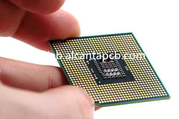
Katika utengenezaji wa vifaa vya kisasa vya elektroniki, PCB (Bodi ya Mzunguko Iliyochapishwa) ni sehemu ya lazima. Katika muundo wa PCB, matumizi ya dhana ya athari za chini na mapungufu inazidi kuwa muhimu. Kupitia uboreshaji wa athari za chini na mapungufu, wiani wa juu wa mzunguko na mpangilio zaidi wa kompakt unaweza kupatikana, na hivyo kuboresha utendaji wa mzunguko na kuegemea. Makala haya yanachunguza dhana hii muhimu na kueleza jinsi ya kufikia utendakazi bora na kutegemewa katika muundo wa PCB.
Ufuatiliaji wa chini ni nini&Kusafisha PCB?
Ufuatiliaji wa chini & Clearance PCB ni dhana muhimu katika muundo wa kisasa wa elektroniki. Inarejelea bodi ya mzunguko iliyochapishwa iliyoundwa na upana wa chini wa mstari na nafasi. Katika muundo wa PCB, upana wa waya na nafasi kati ya waya ni vigezo muhimu, ambayo huathiri moja kwa moja utendaji, kuegemea na gharama ya mzunguko. Kupitia upana wa chini wa mstari na muundo wa nafasi, tunaweza kufikia msongamano wa juu wa mzunguko, mpangilio zaidi wa kompakt, na utendaji bora.
Katika Ufuatiliaji wa Chini & Ubunifu wa PCB wa kibali, upana wa mstari wa chini unarejelea upana wa chini kabisa wa waya kwenye PCB, na nafasi ni umbali wa chini kati ya mistari ya mwongozo. Kawaida, vigezo hivi vinahitaji kudhibitiwa kwa usahihi kulingana na mahitaji maalum ya maombi na michakato ya utengenezaji. Kutumia upana wa chini wa mstari na muundo wa nafasi kunaweza kupunguza njia ya upitishaji wa mawimbi kwenye saketi, na hivyo kupunguza ucheleweshaji na upotezaji wa maambukizi ya ishara na kuboresha kasi ya majibu na utulivu wa mzunguko.
Mbali na kuboresha utendaji wa mzunguko, Ufuatiliaji wa chini&Clearance PCB pia inaweza kuleta faida nyingine nyingi. Kwanza, inaweza kuokoa nafasi ya PCB kwa ufanisi, kuruhusu nyaya zaidi na vipengele kuwekwa katika nafasi ndogo. Hii ni muhimu sana kwa muundo wa bidhaa, hasa kwa bidhaa zilizo na mahitaji ya juu ya miniaturization na ushirikiano wa kazi. Pili, kupitisha upana wa chini wa mstari na muundo wa nafasi pia unaweza kupunguza gharama za utengenezaji wa PCB. Kwa sababu waya na mapungufu kwenye bodi za mzunguko ni ngumu zaidi, vifaa hutumiwa kwa ufanisi zaidi na kuna chakavu kidogo na hasara katika mchakato wa utengenezaji, kusababisha gharama za chini.
Ufuatiliaji wa chini&Clearance PCB ina anuwai ya matumizi katika nyanja mbalimbali. Katika vifaa vya elektroniki vya watumiaji, kama vile simu mahiri, vidonge na vifaa vya nyumbani, muundo wa kompakt na utendaji wa juu ni sababu za kushinda. Katika nyanja kama vile vifaa vya mawasiliano, Vifaa vya matibabu, na mifumo ya udhibiti wa viwanda, uthabiti na kuegemea kwa Ufuatiliaji wa Kima cha Chini & PCB ya kibali ni muhimu sana. Kwa kupitisha upana wa chini wa mstari na muundo wa nafasi, nyaya za kuaminika zaidi na za ufanisi zinaweza kupatikana, kutoa msaada dhabiti na dhamana kwa hali mbali mbali za maombi.
Kukamilisha, Ufuatiliaji wa chini & Clearance PCB ni sehemu ya lazima ya muundo wa kisasa wa kielektroniki. Haiwezi tu kuongeza utendaji wa mzunguko, lakini pia kupunguza gharama na ukubwa, na kuboresha ushindani wa bidhaa na kutegemewa. Kwa kuelewa kwa kina na kutumia kanuni za muundo wa nafasi na upana wa chini zaidi wa mstari, tunaweza kuleta uvumbuzi zaidi na fursa kwa maendeleo ya sekta ya umeme.
Ufuatiliaji wa chini&Mwongozo wa Marejeleo wa muundo wa PCB wa kibali.
Katika uhandisi wa kisasa wa elektroniki, Ufuatiliaji wa chini & Usanifu wa PCB wa kibali umekuwa mojawapo ya mikakati muhimu ya kuboresha utendakazi wa mzunguko na kupunguza gharama na ukubwa. Ili kuwasaidia wahandisi kuelewa na kutumia vyema kanuni hii ya usanifu, hapa chini ni mwongozo wa kina wa kumbukumbu.
Ufuatiliaji wa chini&Clearance PCB inarejelea PCB iliyoundwa na upana wa chini wa mstari na nafasi. Upana wa mstari huongoza upana wa mstari au reli, wakati nafasi inaongoza umbali kati ya mistari au kati ya kondakta na vipengele vingine. Kwa kudhibiti vyema vipimo hivi, kompakt zaidi, miundo ya mzunguko wa utendaji wa juu inaweza kupatikana.
Kuchagua upana wa mstari unaofaa na nafasi ni hatua muhimu katika Ufuatiliaji wa Kiwango cha Chini & Ubunifu wa PCB wa kibali. Uchaguzi wa upana wa mstari unapaswa kuzingatia upakiaji wa sasa, mahitaji ya maambukizi ya ishara na uwezo wa mchakato wa utengenezaji. Uamuzi wa nafasi unahitaji kuzingatia mambo kama vile mwingiliano wa mawimbi, usalama wa umeme, na gharama za utengenezaji.
Katika Ufuatiliaji wa Chini&Ubunifu wa PCB wa kibali, kudumisha uadilifu mzuri wa ishara na utangamano wa sumakuumeme ni muhimu. Upana wa mstari unaofaa na muundo wa nafasi unaweza kupunguza mazungumzo ya mawimbi na usumbufu, na hivyo kuhakikisha utulivu na uaminifu wa mzunguko.
Wahandisi wanapaswa kutumia mbinu bora zaidi na zana za usanifu wa hali ya juu wakati wa kuunda Ufuatiliaji wa Kiwango cha Chini & PCB za kibali. Zana hizi zinaweza kuwasaidia wahandisi kutathmini haraka na kwa usahihi athari ya upana wa mstari na nafasi, kuboresha mpangilio wa mzunguko, na kuboresha ufanisi wa muundo na ubora.
Hatimaye, wabunifu wanapaswa kufuata mahitaji na viwango vya utengenezaji kila wakati wakati wa kuunda Ufuatiliaji wa Kiwango cha Chini & PCB za kibali. Hii ni pamoja na kuhakikisha kuwa upana wa laini na nafasi zinatii mahitaji ya mchakato wa utengenezaji, pamoja na kufikia viwango vinavyofaa vya usalama na uaminifu wa umeme.
Kwa kuelewa kikamilifu na kutumia miongozo iliyo hapo juu, wahandisi wanaweza kubuni utendaji wa juu zaidi, kuegemea juu Kiwango cha chini cha Ufuatiliaji & PCB za kibali, kutoa ufumbuzi wa kuaminika zaidi na ufanisi kwa ajili ya maendeleo ya bidhaa za kisasa za elektroniki.
Ni nyenzo gani inatumika katika Ufuatiliaji wa Kima cha chini cha chini&Kusafisha PCB?
Katika muundo wa Kiwango cha chini cha Ufuatiliaji & Kusafisha PCB, nyenzo zinazotumiwa ni muhimu kwa utendaji wa mzunguko na kuegemea. Ifuatayo ni nyenzo za kawaida zinazotumiwa kwa Ufuatiliaji wa Kima cha Chini & Kusafisha PCB:
Substrate
Nyenzo ya msingi ni nyenzo ya msingi ya PCB, ambayo hutoa msaada wa mitambo na mali ya insulation. Katika Ufuatiliaji wa Chini & Kusafisha PCB, substrates kawaida ni pamoja na FR-4 fiberglass composites. FR-4 ina nguvu bora ya mitambo na mali ya insulation na inaweza kukidhi mahitaji ya muundo wa kompakt.
Foil ya shaba
Foil ya shaba hutumiwa kama safu ya conductive ya mizunguko na inawajibika kwa kupitisha mkondo wa umeme na ishara. Katika Ufuatiliaji wa Chini & Kusafisha PCB, karatasi nyembamba ya shaba kwa kawaida hutumiwa kufikia upana na nafasi ya mstari mdogo. Foil ya shaba ya usafi wa juu hutoa upinzani mdogo na solderability nzuri, kuhakikisha utendaji thabiti wa mzunguko.
Mask ya Solder
Mask ya solder hutumiwa kufunika uso wa PCB na kulinda waya na pedi kutoka kwa mazingira ya nje. Katika Ufuatiliaji wa Chini & Kusafisha PCB, uteuzi wa barakoa ya solder unahitaji kuzingatia upana wa chini wa mstari na mahitaji ya nafasi ili kuhakikisha utendakazi na usahihi wake..
Wino wa Kuchapisha
Wino za uchapishaji hutumiwa kwa kawaida kuchapisha nembo, maandishi na michoro kwenye PCB. Katika Ufuatiliaji wa Chini & Kusafisha PCB, uteuzi wa wino wa uchapishaji pia unahitaji kuzingatia upana wa mstari wa chini na mahitaji ya nafasi ili kuhakikisha uwazi na usahihi wa uchapishaji..
Nyenzo za Usaidizi
Mbali na nyenzo kuu hapo juu, pia kuna baadhi ya vifaa vya msaidizi ambavyo vina jukumu muhimu katika utengenezaji wa Minimum Trace & Kusafisha PCB. Kwa mfano, adhesive conductive hutumiwa kujaza mapengo na mashimo katika nyaya ili kuongeza uunganisho wa mzunguko; foil iliyofunikwa na shaba hutumiwa kuongeza nguvu za mitambo na sifa za conductive za PCB.
Kwa muhtasari, uteuzi wa nyenzo wa Kiwango cha chini cha Ufuatiliaji & PCB ya kibali ina athari muhimu kwa utendaji wa mzunguko na kuegemea. Kwa kuchagua kwa busara na kuboresha nyenzo, tunaweza kuhakikisha kwamba miundo ya PCB inakidhi mahitaji ya chini ya upana wa mstari na nafasi huku ikiboresha utendakazi na uthabiti wa mzunguko.
Ni saizi gani ya Ufuatiliaji wa Chini&Kusafisha PCB?
Wakati wa kuzungumza juu ya Kiwango cha chini cha Ufuatiliaji & PCB za kibali, ukubwa ni kawaida kuamua na mahitaji ya maombi maalum na mapungufu ya teknolojia kutumika. Hata hivyo, tunaweza kutoa miongozo ya jumla ya kuelewa anuwai ya ukubwa wao.
PCB zilizoundwa kwa upana wa chini wa mstari na nafasi kawaida hutumiwa katika hali ambapo kiwango cha juu cha ujumuishaji na muundo wa kompakt inahitajika.. Kwa hiyo, mara nyingi huwa ndogo kwa ukubwa ili kukidhi vikwazo vya nafasi na mahitaji ya utendaji wa bidhaa. Kwa ujumla, saizi ya Kiwango cha chini cha Ufuatiliaji & PCB ya kibali inaweza kuanzia milimita chache za mraba hadi sentimita chache za mraba.
Kwa vifaa vidogo vya kubebeka, kama vile simu mahiri, vidonge, na vifaa vya kushika mkono, Ufuatiliaji wa chini & PCB za kibali kwa kawaida huhitaji saizi ndogo sana ili kukidhi wepesi na kubebeka kwa kifaa.. Katika kesi hizi, PCB inaweza tu kuwa na ukubwa wa milimita chache za mraba, lakini bado inahitaji kudumisha utendaji mzuri na utulivu.
Katika baadhi ya maombi mengine, kama vile mifumo ya udhibiti wa viwanda, Vifaa vya matibabu, na vifaa vya mawasiliano, Kiwango cha chini cha Ufuatiliaji & PCB ya kibali inaweza kuwa kubwa zaidi ili kuchukua saketi na vijenzi zaidi. Lakini hata katika maombi haya, muundo wa kompakt bado ni muhimu kuzingatia kwa sababu huokoa nafasi, inapunguza gharama, na inaboresha uaminifu na uthabiti wa mfumo.
Ikumbukwe kwamba ingawa Minimum Trace & PCB za kibali kwa kawaida huwa ndogo kwa ukubwa, vikwazo vya mchakato wa utengenezaji na upatikanaji wa nyenzo bado unahitaji kuzingatiwa wakati wa mchakato wa kubuni. Kwa hiyo, wakati wa kupima PCB, wahandisi wa kubuni wanahitaji kusawazisha utendaji kwa uangalifu, gharama na uwezekano wa utengenezaji ili kuhakikisha ubora na uaminifu wa bidhaa ya mwisho.
Kwa muhtasari, Ufuatiliaji wa chini & Saizi za PCB za kibali kwa kawaida ni ndogo, lakini hutofautiana kulingana na mahitaji maalum ya maombi na vikwazo vya kiufundi. Kupitia muundo na uboreshaji unaofaa, tunaweza kuhakikisha kuwa PCB bado ina utendakazi mzuri na uthabiti huku ikiwa ndogo kwa ukubwa, hivyo kukidhi mahitaji ya vifaa vya kisasa vya kielektroniki.
Mchakato wa Mtengenezaji wa Ufuatiliaji wa Kima cha Chini&Kusafisha PCB.
Tunapozungumza juu ya upana wa mstari wa chini na PCB ya nafasi, ni muhimu kuelewa mchakato wa utengenezaji wake. Kutengeneza Ufuatiliaji wa Kiwango cha Chini & Uondoaji wa PCB unahitaji mfululizo wa hatua ngumu na michakato sahihi ili kuhakikisha kuwa bidhaa ya mwisho inakidhi mahitaji ya muundo na viwango vya ubora wa juu..
Uthibitishaji wa muundo na uboreshaji
Hatua ya kwanza katika utengenezaji wa Minimum Trace & Clearance PCB ni uthibitishaji wa muundo na uboreshaji. Wakati wa awamu ya kubuni, wahandisi lazima wazingatie mambo kama vile upana wa mstari, nafasi, Uadilifu wa ishara, nk., na utumie programu ya CAD kwa muundo. Uthibitishaji wa muundo unakusudiwa kuhakikisha kuwa mpangilio wa PCB unatii vipimo na unakidhi mahitaji ya utendaji. Katika hatua hii, marudio mengi na uboreshaji huenda ukahitajika ili kufikia athari bora ya muundo.
Maandalizi ya substrate
Mara tu muundo utakapokamilika na kuthibitishwa, hatua inayofuata ni maandalizi ya substrate. Sehemu ndogo kawaida hutengenezwa kwa nyenzo za mchanganyiko wa fiberglass (kama FR-4), ambayo hutoa msaada wa kimsingi wa kimuundo wa PCB. Wakati wa kuandaa substrate, unahitaji kuhakikisha kuwa uso wake ni laini, gorofa, na inakidhi mahitaji ya ukubwa wa kawaida kwa utengenezaji wa PCB.
Kifuniko cha foil ya shaba
Foil ya shaba ni safu kuu ya conductive ya PCB na inawajibika kwa kuunganisha vipengele mbalimbali katika mzunguko. Wakati wa mchakato wa utengenezaji, foil ya shaba imefunikwa juu ya uso wa substrate, na kisha teknolojia ya etching ya kemikali hutumiwa kuondoa foil ya shaba iliyozidi kulingana na mahitaji ya muundo, kuacha mistari na mapungufu yanayohitajika.
Uongofu wa picha
Ugeuzaji wa picha ni mchakato wa kubadilisha michoro ya muundo wa PCB kuwa ubao halisi wa PCB. Kwa kuhamisha picha ya kubuni kwenye uso wa substrate ya shaba iliyofunikwa na foil, waya na mapengo kwenye ubao wa PCB, pamoja na miundo au vipengele vingine maalum, inaweza kufafanuliwa kwa usahihi.
Plating
Electroplating ni moja ya hatua muhimu katika mchakato wa utengenezaji wa PCB. Inatumika kuongeza mali ya conductive ya uso wa PCB. Kwa kuzamisha PCB katika suluhisho iliyo na ioni za chuma, safu ya kifuniko cha chuma sare inaweza kuundwa kwenye uso wa PCB ili kuongeza conductivity na upinzani wa kutu wa mzunguko..
Chanjo ya mask ya solder
Ufunikaji wa mask ya solder ni kulinda uso wa PCB kutoka kwa mazingira ya nje na kuboresha kuegemea na uimara wa PCB.. Katika hatua hii, mapengo kati ya waya na mapengo yanajazwa na uso wa PCB unalindwa kutokana na mzunguko mfupi au kutu kwa kuifunika kwa safu ya resin ya thermoset..
Mkutano wa mwisho na upimaji
Hatimaye, Kiwango cha chini cha Ufuatiliaji kilichokamilika & PCB ya kibali itatumwa kwa warsha ya kusanyiko kwa mkusanyiko na majaribio ya mwisho. Katika hatua hii, PCB itaunganishwa na vifaa vingine vya kielektroniki (kama vile chips, wapinzani, capacitors, nk.), na upimaji wa utendakazi na uthibitishaji wa utendakazi utafanywa ili kuhakikisha utendakazi wa kawaida wa PCB na kukidhi mahitaji ya muundo.
Kupitia hatua hapo juu, upana wa chini wa mstari na nafasi PCB hupitia mchakato sahihi na changamano wa utengenezaji, hatimaye kuzalisha ubora wa juu, Bidhaa za elektroniki za utendaji wa juu. PCB hizi zinatumika sana katika nyanja mbalimbali, kutoa msaada mkubwa na dhamana kwa maendeleo ya teknolojia ya kisasa.
Eneo la Maombi la Ufuatiliaji wa Kima cha Chini&Kusafisha PCB.
Katika muundo wa kisasa wa elektroniki, Ufuatiliaji wa chini & Teknolojia ya PCB ya kibali ina anuwai ya matumizi. Faida zake hazionyeshwa tu katika kuboresha utendaji wa mzunguko na kupunguza gharama na ukubwa, lakini pia katika kunyumbulika na kutegemewa kwake kuhusika katika nyanja mbalimbali. Yafuatayo ni matumizi ya Kiwango cha chini cha Ufuatiliaji&Kibali PCB katika nyanja kadhaa kuu:
Bidhaa za kielektroniki za watumiaji
Katika uwanja wa matumizi ya umeme, kama vile simu mahiri, vidonge, kamera za digital, nk., mahitaji ya ukubwa wa bidhaa na utendaji yanazidi kuongezeka. Muundo thabiti na vipengele vya utendaji wa juu vya Ufuatiliaji wa Kiwango cha Chini&PCB za kibali huwafanya kuwa bora kwa bidhaa hizi. Kwa kutumia upana wa chini wa mstari na miundo ya nafasi, msongamano wa juu wa mzunguko unaweza kufikiwa ili kushughulikia utendakazi na vijenzi zaidi katika nafasi ndogo huku kukiwa na utendakazi wa bidhaa na kutegemewa..
Kifaa cha mawasiliano
Katika uwanja wa vifaa vya mawasiliano, kama vile vituo vya msingi, Njia, swichi, nk., Ufuatiliaji wa chini & Clearance PCB pia inatumika sana. Vifaa hivi vinahitaji muundo wa mzunguko wa utendaji wa juu ili kuhakikisha mawimbi thabiti ya mawasiliano na upitishaji wa data, huku pia ikihitaji miundo thabiti ili kukidhi mahitaji ya ukubwa wa kifaa. Kupitisha upana wa chini wa laini na muundo wa nafasi kunaweza kuboresha kasi na uthabiti wa utumaji wa mawimbi huku ukipunguza mwingiliano wa sumakuumeme na mazungumzo ya mawimbi., na hivyo kuboresha utendaji na uaminifu wa vifaa vya mawasiliano.
Vifaa vya matibabu
Katika uwanja wa vifaa vya matibabu, kama vile pacemaker, vyombo vya ufuatiliaji wa matibabu, nk., kuna mahitaji ya juu sana ya kuaminika na utulivu wa muundo wa mzunguko. Muundo ulioboreshwa wa Ufuatiliaji wa Kiwango cha Chini&PCB ya kibali inaweza kuhakikisha uthabiti na uaminifu wa mzunguko, huku pia ikikidhi mahitaji madhubuti ya saizi na uzito wa vifaa vya matibabu. Vifaa hivi mara nyingi vinahitaji kuunganishwa kwa kazi nyingi na sensorer katika nafasi ndogo, na kubuni kwa upana mdogo wa mstari na nafasi inaweza kusaidia kufikia lengo hili.
Mfumo wa udhibiti wa viwanda
Katika uwanja wa mifumo ya udhibiti wa viwanda, kama vile PLC (kidhibiti cha mantiki kinachoweza kupangwa), mitandao ya sensor, nk., Ufuatiliaji wa chini & Clearance PCB pia inatumika sana. Mifumo hii inahitaji muundo wa mzunguko wa juu wa utendaji ili kuhakikisha utulivu na uaminifu wa mchakato wa uzalishaji wa viwanda, huku pia ikihitaji miundo thabiti ili kuendana na mahitaji ya mazingira ya viwanda. Kupitisha upana wa chini wa mstari na muundo wa nafasi kunaweza kuboresha uwezo wa kuzuia mwingiliano na kutegemewa kwa saketi, na pia inaweza kupunguza matumizi ya nishati na gharama ya matengenezo ya mfumo, na hivyo kuboresha utendaji wa jumla na kutegemewa kwa mfumo wa udhibiti wa viwanda.
Kukamilisha, matumizi ya Kiwango cha chini cha Ufuatiliaji & Clearance PCB teknolojia katika nyanja za matumizi ya umeme, vifaa vya mawasiliano, vifaa vya matibabu na mifumo ya udhibiti wa viwanda hutoa ufumbuzi wa kuaminika na ufanisi kwa ajili ya maendeleo ya viwanda hivi. Na maendeleo endelevu na uvumbuzi wa teknolojia, Ninaamini kuwa Ufuatiliaji wa Chini & Teknolojia ya PCB ya kibali itaonyesha uwezo wake mkubwa na thamani katika nyanja zaidi.
Je, ni faida gani za Kima cha chini cha Ufuatiliaji&Kusafisha PCB?
Tunapozungumza juu ya Ufuatiliaji wa Kiwango cha chini & Kusafisha PCB, hatuzungumzii tu kipengele kimoja cha muundo wa mzunguko, lakini falsafa ya kubuni ambayo huleta faida nyingi kwa vifaa vya kisasa vya kielektroniki. Zifuatazo ni faida za upana wa chini wa mstari na nafasi ya PCB:
Kuboresha utendaji wa mzunguko
Ufuatiliaji wa chini&Ubunifu wa PCB wa kibali hufanya njia ya upitishaji wa mawimbi kwenye saketi kuwa ngumu zaidi na bora kwa kupunguza upana wa laini na nafasi.. Uboreshaji huu unaweza kupunguza ucheleweshaji na upotoshaji wa usambazaji wa mawimbi, na hivyo kuboresha utendaji na kasi ya majibu ya mzunguko. Faida hii ni dhahiri hasa kwa maombi ya juu-frequency.
Boresha utumiaji wa nafasi
Katika vifaa vya kisasa vya elektroniki, nafasi mara nyingi ni rasilimali ya anasa. Kiwango cha chini cha Ufuatiliaji & Usanifu wa PCB wa kibali unaweza kufikia utendaji na utendaji zaidi katika nafasi ndogo. Kubuni kwa upana mdogo wa mstari na nafasi huruhusu mpangilio thabiti zaidi, kuacha nafasi zaidi kwa vipengele vingine na utendaji.
Punguza gharama
Huku mahitaji ya vifaa vya kielektroniki yanavyoendelea kuongezeka, kupunguza gharama imekuwa moja ya malengo ya juu ya wazalishaji. Matumizi ya Kiwango cha chini cha Ufuatiliaji & Ubunifu wa PCB wa kibali unaweza kusaidia watengenezaji kupunguza gharama za nyenzo, gharama za uzalishaji na matengenezo. Muundo wa kompakt unamaanisha upotezaji mdogo wa nyenzo, huku pia kupunguza utata na gharama katika mchakato wa uzalishaji.
Kuboresha kuegemea
Katika vifaa vya elektroniki, kuegemea ni muhimu. Ufuatiliaji wa chini&Usanifu wa PCB wa kibali unaweza kusaidia kuboresha uthabiti na kutegemewa kwa saketi. Kupitia upana wa chini wa mstari na muundo wa nafasi, kuingiliwa na kelele katika mzunguko inaweza kupunguzwa, na hivyo kupunguza uwezekano wa kushindwa na kupanua maisha ya huduma ya vifaa.
Rahisi zaidi kutekeleza kazi ngumu
Huku kazi za vifaa vya kielektroniki zinavyoendelea kuongezeka, kubuni mzunguko inakuwa ngumu zaidi na zaidi. Ufuatiliaji wa chini&Usanifu wa PCB wa kibali unaweza kusaidia wahandisi kufikia kazi na utendakazi changamano zaidi. Muundo wa kompakt unamaanisha njia fupi za upitishaji wa mawimbi na ucheleweshaji mdogo wa mzunguko, kuifanya iwe rahisi kutekeleza kazi za utendaji wa juu.
Kwa jumla, Ufuatiliaji wa chini&Ubunifu wa PCB wa kibali hauwezi tu kuboresha utendaji wa mzunguko na kuegemea, lakini pia kupunguza gharama na ukubwa, hivyo kutoa suluhisho la kuaminika zaidi na la ufanisi kwa ajili ya maendeleo ya vifaa vya kisasa vya elektroniki.
Maswali
Ni nyanja zipi za maombi ambazo ni Ufuatiliaji wa Chini&Kibali PCB kufaa kwa?
Ufuatiliaji wa chini&Clearance PCB inafaa kwa nyanja mbalimbali, pamoja na umeme wa watumiaji, vifaa vya mawasiliano, Vifaa vya matibabu, na mifumo ya udhibiti wa viwanda. Katika matumizi haya, utendaji wa juu na muundo wa kompakt ni muhimu, na upana wa chini wa mstari na muundo wa nafasi ni muhimu ili kukidhi mahitaji haya.
Ni mambo gani yanapaswa kuzingatiwa wakati wa kuunda Ufuatiliaji wa Kiwango cha chini&Kusafisha PCB?
Wakati wa kubuni Kiwango cha chini cha Ufuatiliaji & Kusafisha PCB, mambo mengi yanapaswa kuzingatiwa, kama vile uadilifu wa ishara, Utangamano wa umeme, Mchakato wa utengenezaji, nk. Kukubali mbinu bora na kuzingatia kwa karibu maelezo ni ufunguo wa kuhakikisha muundo uliofanikiwa.
Jinsi ya kuhakikisha kuegemea kwa Ufuatiliaji wa Kiwango cha Chini&Kusafisha PCB?
Ili kuhakikisha kuegemea kwa Ufuatiliaji wa Kiwango cha Chini & Kusafisha PCB, uthibitishaji mkali wa muundo, udhibiti wa mchakato wa utengenezaji na ukaguzi wa ubora unahitajika. Wakati huo huo, kuchagua nyenzo za ubora wa juu na michakato inayofaa ya utengenezaji pia ni mambo muhimu katika kuhakikisha kuegemea.
Je, upana wa mstari wa chini zaidi na muundo wa nafasi utakuwa na athari gani kwenye mchakato wa utengenezaji wa PCB?
Upana wa chini wa mstari na muundo wa nafasi una athari muhimu kwenye mchakato wa utengenezaji wa PCB. Inahitaji watengenezaji kuwa na usahihi wa juu na kiwango cha kiufundi ili kuhakikisha utengenezaji wa bodi za PCB zinazokidhi mahitaji ya muundo. Kwa hiyo, wakati wa kuchagua mtengenezaji wa PCB, mtu anapaswa kuzingatia uwezo wake wa utengenezaji na uzoefu.