CO., LTD")
Que sont les substrats SHDBU?
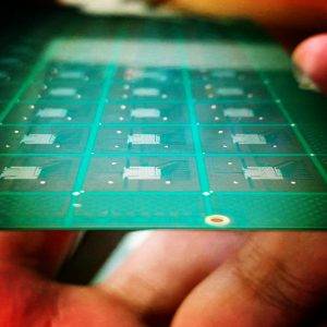
Fabrication de substrats SHDBU. Nous pouvons produire le meilleur pas de bosse le plus samlle avec 100um, La meilleure trace la plus petite est 9UM. et le plus petit écart est de 9 um. la plupart des modèles ont une trace et un espacement de 15 um à 30 um.
Substrats SHDBU, nom complet Substrats reconstituants à très haute densité, est une technologie de pointe accrocheuse dans le circuit imprimé actuel (PCB) champ.
L'introduction de cette technologie met en évidence les progrès innovants de PCB ingénierie et offre aux fabricants des options de conception plus flexibles et plus puissantes.
Parmi ces substrats, le concept de conception de super haute densité permet d'obtenir une densité de composants supérieure en empilant étroitement plusieurs couches de composants de circuit. Cela permet d'intégrer davantage de composants électroniques dans un espace limité, offrant une plus grande liberté dans la taille et le poids des produits électroniques.
Le rôle clé de ces substrats dans l’électronique moderne se reflète dans les performances supérieures qu’ils offrent. Les substrats SHDBU excellent dans leurs propriétés électriques et thermiques, fournir une base solide pour les circuits intégrés (CI) et autres composants électroniques. Sa conductivité thermique élevée garantit un fonctionnement stable des appareils électroniques dans des applications à charge élevée et à haute fréquence.
En outre, Les substrats SHDBU offrent de nouvelles possibilités pour la conception compacte des produits électroniques. Cette technologie de substrat avancée permet aux produits électroniques d'être plus petits et plus légers que les cartes de circuits imprimés traditionnelles sans compromettre les performances..
Dans l'ensemble, l'émergence des substrats SHDBU représente une révolution dans le domaine de l'ingénierie des PCB. En alliant performances supérieures et conception compacte, cette technologie de pointe entraîne de nouveaux développements dans la fabrication d'appareils électroniques, jeter les bases de produits électroniques plus avancés et plus efficaces à l'avenir. L'application des substrats SHDBU indique que même si le domaine électronique explore constamment l'innovation, c'est aussi améliorer constamment les performances et la fiabilité des produits.
Substrats SHDBU
Quelles sont les fonctions des substrats SHDBU?
Cette fonctionnalité est obtenue grâce à une excellente conductivité électrique et thermique, ce qui rend les substrats SHDBU idéaux pour obtenir des performances optimales dans les applications exigeantes.
Dans les conceptions haute densité, Les substrats SHDBU se démarquent, permettant l'intégration d'un grand nombre de composants dans un espace limité. Cette propriété est cruciale pour la miniaturisation et l’allègement des appareils électroniques modernes. Par rapport aux substrats traditionnels, Les substrats SHDBU permettent une intégration plus compacte et plus efficace des composants électroniques grâce à leurs capacités d'empilage ultra haute densité, offrant la possibilité d'optimiser la taille et le poids des appareils.
D'un point de vue électrique, les excellentes performances des substrats SHDBU garantissent la stabilité et la fiabilité de la transmission du signal. Ceci est crucial pour les scénarios d’application exigeants tels que les équipements de communication, équipement médical, et systèmes de conduite autonome. La conductivité thermique des substrats SHDBU est également l'une de ses caractéristiques frappantes. Dans les appareils électroniques modernes, une meilleure dissipation de la chaleur est essentielle, et la conception des substrats SHDBU permet de gérer et de dissiper la chaleur plus efficacement dans des espaces limités.
Dans l'ensemble, Les substrats SHDBU sont idéaux pour les hautes performances d'aujourd'hui, conceptions de dispositifs électroniques à haute densité en fournissant une base solide pour les composants électroniques et une excellente conductivité électrique et thermique. Ses performances supérieures dans la configuration des circuits intégrés et d'autres composants clés auront un impact profond sur le développement de la future technologie électronique.. Comme l'une des innovations de pointe en matière d'ingénierie des PCB, Les substrats SHDBU contribuent à orienter les appareils électroniques vers un format plus petit, un avenir plus puissant et plus efficace.
Quels types de substrats SHDBU existe-t-il?
En ingénierie PCB, Substrats SHDBU, comme un développement innovant, ne diffèrent pas seulement par leur structure et leurs performances, mais sont également divisés en plusieurs types en fonction des applications spécifiques et des exigences de performances, offrant une plus grande flexibilité et adaptabilité à la conception électronique. sexe. Voici les types courants de substrats SHDBU:
SHDBU monocouche
Les substrats SHDBU monocouches ont une conception monocouche simple sur la structure du substrat et conviennent aux applications nécessitant peu d'espace mais des exigences de performances élevées.. Sa conception épurée en fait un choix léger et économique, en particulier dans les domaines ayant des exigences particulières en matière de flexibilité et de légèreté.
SHDBU multicouche
Les substrats SHDBU multicouches sont une conception plus complexe qui permet d'obtenir une densité d'intégration de composants plus élevée grâce à une structure empilée multicouche. Ce type convient aux applications où l'espace est limité mais où un grand nombre de composants doivent être intégrés, fournir un support plus puissant pour les appareils électroniques hautes performances.

Substrats SHDBU
SHDBU hybride
Les substrats hybrides SHDBU combinent les avantages du monocouche et du multicouche, offrir aux designers une plus grande liberté. Ce type de substrat répond aux exigences de haute densité tout en équilibrant les exigences de flexibilité et d'intégrité du signal.. Les substrats hybrides SHDBU conviennent à une variété de scénarios d'application en raison de leur flexibilité.
Chaque type de substrats SHDBU offre des avantages uniques en termes de flexibilité, intégrité du signal et gestion thermique. En termes de flexibilité, ils peuvent s'adapter à des conceptions de différentes formes et courbures, offrant une plus grande liberté pour les applications spéciales. En termes d'intégrité du signal, une structure empilée haute densité aide à réduire les interférences électromagnétiques dans la transmission du signal et à améliorer la qualité du signal. En termes de gestion thermique, ces différents types de substrats SHDBU dispersent et conduisent efficacement la chaleur à travers des structures d'empilement optimisées pour garantir le fonctionnement stable des composants électroniques.
Dans l'ensemble, les différents types de substrats SHDBU offrent aux ingénieurs davantage d'options à personnaliser en fonction des besoins spécifiques du projet et des exigences de performances. Que ce soit dans les domaines de haute technologie qui recherchent la performance ultime, ou dans les domaines qui nécessitent une légèreté et une flexibilité plus élevées, Les substrats SHDBU ont démontré une excellente adaptabilité et performance. Cela en fait une technologie clé indispensable dans la conception électronique moderne..
Quelle est la différence entre les substrats SHDBU et les PCB traditionnels?
Dans le domaine de l'ingénierie PCB, Les substrats SHDBU présentent des innovations accrocheuses par rapport aux cartes de câblage imprimées traditionnelles (PWB) et cartes de circuits imprimés (PCBS). Bien que les PWB et PCB traditionnels jouent un rôle important en tant qu'éléments constitutifs des appareils électroniques, Les substrats SHDBU ont apporté des avancées significatives en matière de conception grâce à leurs caractéristiques uniques.
D'abord, Les substrats SHDBU stimulent les progrès de la conception en offrant une densité de composants plus élevée et des capacités de transmission de signal améliorées. Par rapport aux substrats traditionnels, Les substrats SHDBU ont d'excellentes capacités d'empilage, permettant à davantage de composants d'être intégrés de manière plus compacte dans un espace limité. L'innovation dans cette technologie apporte une plus grande flexibilité à la conception des appareils électroniques et peut répondre plus efficacement aux besoins des produits électroniques modernes pour les petits, léger et performant.
En termes de conception de la carte mère, Les substrats SHDBU offrent aux fabricants plus de place à la créativité. En utilisant cette technologie de substrat avancée, les fabricants sont capables de concevoir des configurations plus compactes et plus efficaces, contribuer à la miniaturisation de l’ensemble des appareils électroniques. Les caractéristiques haute densité des substrats SHDBU offrent davantage d'options de configuration pour les cartes mères, permettant aux appareils électroniques de s'adapter plus facilement aux exigences de taille réduite tout en conservant leurs performances.
Comparé aux PCB de type substrat (Orthophonistes), Les substrats SHDBU présentent des avantages en termes de capacités d'empilage. Malgré leurs similitudes, Les substrats SHDBU permettent d'intégrer des circuits plus complexes dans un encombrement réduit en offrant de plus grandes capacités d'empilage. Cela donne aux concepteurs une plus grande liberté pour être plus innovants dans la disposition et l'interconnexion des composants électroniques..
Par rapport à l'interconnexion haute densité (HDI) substrats, Les substrats SHDBU poussent encore la technologie vers de nouveaux sommets. Bien qu'ils soient étroitement liés, Les substrats SHDBU améliorent considérablement les performances des appareils électroniques en permettant des niveaux de densité et de fonctionnalité sans précédent.. Cette innovation rend non seulement les appareils électroniques plus compacts, mais atteint également des performances supérieures dans la transmission du signal, gestion thermique, etc..
En résumé, Les substrats SHDBU sont devenus une technologie révolutionnaire dans le domaine de l'ingénierie des PCB grâce à leurs excellentes performances et leur flexibilité de conception avancée.. En optimisant la densité des composants et les capacités de transmission du signal, ainsi que d'apporter des contributions uniques à la conception de cartes mères, capacités d'empilage, etc., Les substrats SHDBU ouvrent de nouvelles possibilités pour le développement des futurs appareils électroniques.
Quelle est la structure et la technologie de production des substrats SHDBU?
La structure des substrats SHDBU constitue une représentation exemplaire de l'ingénierie moderne des cartes de circuits imprimés., transcendant la simple superposition de matériaux pour incarner une application ingénieuse de composants de haute qualité. En son coeur, cette structure comporte des matériaux isolants avancés et des couches conductrices finement empilées pour créer un système sophistiqué.
En particulier, l'importance des matériaux isolants avancés est primordiale dans la formation de la structure du substrat SHDBU. Ces matériaux présentent non seulement des propriétés isolantes exceptionnelles, mais démontrent également une résilience face aux conditions extrêmes., y compris les températures et l'humidité élevées. Cette sélection minutieuse des matériaux garantit que les substrats SHDBU maintiennent des performances stables et fiables dans divers scénarios environnementaux..
Deuxièmement, le choix de la couche conductrice affecte directement les propriétés électriques des substrats SHDBU. Ces couches conductrices sont conçues et traitées avec précision pour garantir que le courant peut être transmis efficacement dans toute la structure et réduire la perte de signal.. Cette conception prend en compte les exigences de haute efficacité et de haute fiabilité des appareils électroniques modernes, permettant aux substrats SHDBU de maintenir d'excellentes performances électriques même dans des configurations denses.
Cette structure complexe soigneusement conçue est un facteur clé pour permettre aux substrats SHDBU d'atteindre une densité ultra-élevée.. La sélection et la disposition de chaque couche de matériaux sont soigneusement calculées pour garantir que davantage de composants électroniques peuvent être logés dans un espace limité., offrant la possibilité de miniaturisation et de hautes performances des équipements électroniques modernes.
P.technologie de production
La fabrication de substrats SHDBU implique plusieurs technologies de production clés, et l'innovation continue de ces technologies stimule le développement de substrats SHDBU.
D'abord, technologie de fabrication HDI améliorée (Interconnexion haute densité) est une partie importante de la fabrication des substrats SHDBU. En utilisant des équipements et des processus de fabrication avancés, les fabricants sont en mesure d'obtenir des caractéristiques plus fines et des densités intercouches plus élevées. Les progrès continus de cette technologie permettent aux substrats SHDBU d'accueillir plus de couches dans un encombrement réduit., améliorer les performances globales du conseil d'administration.
Deuxièmement, la méthode semi-additif innovante offre une autre possibilité pour la fabrication de substrats SHDBU. Par rapport aux méthodes additives traditionnelles, cette méthode réduit certaines étapes du processus de fabrication, améliorant ainsi l'efficacité de la fabrication. Cette technologie de production innovante permet aux fabricants de répondre avec plus de flexibilité aux demandes du marché tout en maintenant une qualité et une efficacité élevées..
La combinaison de ces technologies de production apporte un soutien solide à la fabrication de substrats SHDBU, leur permettant de jouer un rôle exceptionnel en haute densité, conceptions électroniques hautes performances.
Dans l'ensemble, la fusion ultime des substrats SHDBU’ la structure et la technologie de production reflètent l'innovation de pointe dans l'ingénierie des cartes de circuits imprimés. Cette conception très complexe et sophistiquée favorise non seulement le développement d'équipements électroniques modernes, mais constitue également une base solide pour les progrès futurs de la technologie électronique.
FAQ sur les substrats SHDBU
Quelle est la différence entre les substrats SHDBU et les substrats traditionnels?
Les substrats SHDBU sont très différents des substrats traditionnels. Les substrats traditionnels sont limités en termes de densité de composants et de transmission du signal, tandis que les substrats SHDBU utilisent une technologie d'empilement ultra haute densité pour accueillir plus de composants dans un espace plus petit., amélioration des performances globales.
Les substrats SHDBU sont-ils adaptés aux applications haute fréquence?
Oui, Les substrats SHDBU conviennent parfaitement aux applications haute fréquence. Ses matériaux et sa conception avancés garantissent une excellente intégrité du signal dans les environnements à haute fréquence, ce qui le rend idéal pour gérer des circuits complexes et des communications haute fréquence.
En quoi les substrats SHDBU sont-ils différents des autres substrats haute densité?
Les substrats SHDBU ont des capacités d'empilement plus avancées que les autres substrats haute densité. Sa structure et sa technologie de fabrication permettent la conception de tailles plus petites, une intégration plus élevée, et circuits plus complexes, jouant ainsi un rôle clé dans les appareils électroniques modernes.
Quelle est la particularité de la technologie de fabrication des substrats SHDBU?
La technologie de fabrication des substrats SHDBU comprend une technologie de fabrication HDI améliorée et une méthode semi-additif innovante. L'introduction de ces technologies permet aux fabricants d'obtenir des fonctionnalités plus fines et une plus grande précision de fabrication pour répondre à la demande croissante en matière de conception d'appareils électroniques..
Les substrats SHDBU sont-ils adaptés à une production à grande échelle?
Oui, Les substrats SHDBU sont déjà largement utilisés dans la production de masse. La maturité et l'efficacité de sa technologie de fabrication en font une option viable pour répondre aux besoins industriels, assurer la fiabilité et les performances des produits électroniques.