주식회사")
RF 패키지 기판 제조업체.RF 패키지 기판 RF 애플리케이션용 고성능 기판 생산 전문 제조업체, 효율적인 신호 전송 및 우수한 열 관리 가능. 진보된 제작 기술로, 그들은 통신의 엄격한 요구를 충족시키기 위해 맞춤형 솔루션을 제공합니다., 항공우주, 방위 산업. 그들의 전문 지식은 중요한 RF 시스템의 신뢰성과 향상된 성능을 보장합니다..
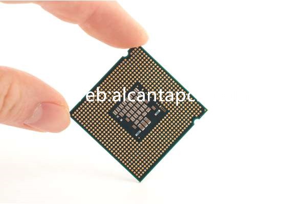
RF (무선 주파수) 패키지 기판 무선 주파수에서 작동하는 전자 장치 제조에 필수적인 구성 요소입니다., 무선 통신 시스템을 포함한, 레이더, 위성 통신. 이 기판은 탁월한 신호 무결성을 제공하도록 설계되었습니다., 열 관리, 기계적 안정성, 고주파 애플리케이션에 이상적입니다.. 이 기사에서는 기능을 살펴봅니다., 디자인 고려 사항, 재료, 제조 공정, 애플리케이션, RF 패키지 기판의 장점.
RF 패키지 기판이란??
RF 패키지 기판은 RF 전자 부품 패키징에 사용되는 특수 소재입니다.. 다양한 전자 장치를 장착하고 상호 연결하는 기반 역할을 합니다., 집적회로 포함 (IC), 저항, 커패시터, 및 인덕터. 이 기판은 신호 손실과 왜곡을 최소화하도록 설계되었습니다., 효율적인 열 관리 보장, 기계적 지원을 제공합니다.. 이는 RF 시스템의 성능과 신뢰성을 유지하는 데 중요합니다..
RF 패키지 기판에 대한 설계 고려 사항
RF 패키지 기판 설계에는 몇 가지 중요한 고려 사항이 포함됩니다.:
적절한 유전 특성을 지닌 올바른 재료 선택, 열전도도, 최적의 성능을 위해서는 기계적 강도가 중요합니다..
과열을 방지하고 안정적인 작동을 보장하려면 효율적인 열 관리가 필수적입니다.. 여기에는 열 비아 통합이 포함됩니다., 히트 스프레더, 및 기타 냉각 메커니즘.
고주파에서 신호 무결성을 유지하려면 미량 임피던스를 신중하게 제어해야합니다., Crosstalk 최소화, 효과적인 접지 및 차폐 기술 구현.
기판은 제조 공정 및 작동 조건을 견딜 수 있을 만큼 충분한 기계적 강도와 안정성을 가져야 합니다., 열 순환 및 기계적 응력 포함.
표면 마감은 부품의 적절한 접착 및 정렬을 보장하고 신호 손실 및 반사를 최소화하기 위해 매끄럽고 결함이 없어야 합니다..
RF 패키지 기판에 사용되는 재료
RF 패키지 기판 제조에는 여러 가지 재료가 일반적으로 사용됩니다.:
알루미나 등의 재료 (Al2O3), 질화알루미늄 (AlN), 및 산화베릴륨 (베오) 우수한 유전 특성과 높은 열 전도성 제공.
고주파 라미네이트, PTFE와 같은 (폴리테트라플루오로에틸렌) 및 세라믹 충전 PTFE 복합재, 낮은 유전 상수 및 손실 탄젠트 값 제공, 최소한의 신호 손실 보장.
구리 및 기타 금속 합금은 우수한 전기 전도성과 신뢰성으로 인해 전도성 트레이스 및 비아에 사용됩니다..
고성능 에폭시 수지는 기판의 층을 서로 접착하기 위한 접착 재료로 사용됩니다., 기계적 강도와 안정성을 제공합니다.
이들은 납땜 가능성을 향상시키고 산화로부터 보호하기 위해 접점 패드에 적용됩니다..
RF 패키지 기판 제조 공정
RF 패키지 기판의 제조 공정에는 몇 가지 정확한 단계가 포함됩니다.:
원료, 고성능 세라믹을 포함한, 유기 라미네이트, 및 금속 합금, 시트 나 필름으로 준비되고 처리됩니다.
기판 재료의 다중 층이 함께 적층되어 축적 구조를 형성합니다.. 이 과정은 층을 결합하기 위해 열과 압력을 가하는 것이 포함됩니다..
회로 패턴은 포토 리소그래피 프로세스를 사용하여 생성됩니다. 감광성 필름 (포토 레지스트) 기판에 적용됩니다, 자외선에 노출됩니다 (UV) 마스크를 통해 빛, 원하는 회로 패턴을 나타 내기 위해 개발되었습니다. 이어서, 기판을 에칭하여 원치 않는 재료를 제거한다.
VIAS는 기판으로 뚫어 서로 다른 층간에 수직 전기 연결을 생성합니다.. 그런 다음이 구멍은 구리로 도금되어 전도성 경로를 설정합니다..
매끄러운, 부품의 적절한 접착 및 정렬을 보장하기 위해 결함 없는 표면 마감이 접촉 패드에 적용됩니다., 신호 손실과 반사를 최소화할 뿐만 아니라.
완성된 기판은 전기 성능에 필요한 사양을 충족하는지 확인하기 위해 엄격한 테스트와 검사를 거칩니다., 신호 무결성, 신뢰성.
RF 패키지 기판의 응용
RF 패키지 기판은 광범위한 고주파 응용 분야에 사용됩니다.:
이 기판은 휴대폰의 RF 부품 패키징을 지원합니다., 기지국, Wi-Fi 라우터, 및 기타 무선 통신 장치.
RF 패키지 기판은 자동차에 사용되는 레이더 시스템에 사용됩니다., 비행, 및 국방 애플리케이션, 고주파수 작동과 신뢰성이 중요한 곳.
이 기판은 위성 통신 시스템에 사용됩니다., 위성 트랜스폰더 및 지상국 장비 포함, 높은 신호 무결성 및 성능 보장.
RF 패키지 기판은 의료기기 및 장비에 활용됩니다., MRI 장비, 무선 환자 모니터링 시스템 등, 안정적인 고주파 작동이 필수적인 곳.
기판은 항공우주 및 방위 산업에 사용됩니다., 통신 시스템을 포함한, 전자전, 및 안내 시스템, 강력한 성능과 신뢰성이 요구되는 곳.
RF 패키지 기판의 장점
RF 패키지 기판은 여러 가지 장점을 제공합니다.:
낮은 유전 상수와 손실 탄젠트 값은 신호 손실과 왜곡을 최소화합니다., 높은 신호 충실도와 성능 유지.
열전도율이 높은 소재로 효율적인 방열 효과 제공, 과열을 방지하고 안정적인 작동을 보장합니다..
기판은 견고한 기계적 지지력을 제공합니다., 다양한 환경 조건에서 패키지 구성 요소의 신뢰성과 내구성 보장.
RF 패키지 기판은 광범위한 RF 구성 요소와 호환되며 다양한 장착 및 상호 연결 기술을 수용할 수 있습니다..
이러한 기판은 특정 설계 요구 사항을 충족하도록 맞춤 설정할 수 있습니다., 특정 재료의 통합을 포함하여, 레이어 구성, 및 표면 마감.
FAQ
RF 패키지 기판 사용의 주요 이점은 무엇입니까??
주요 이점은 높은 신호 무결성을 포함합니다., 효율적인 열 관리, 기계적 안정성, RF 부품과의 호환성, 및 맞춤화 가능성. 이러한 기판은 안정적인 신호 무결성과 효율적인 열 관리 기능을 갖춘 고성능 RF 전자 장치 제조를 위한 기반을 제공합니다..
RF 패키지 기판에 일반적으로 사용되는 재료는 무엇입니까??
일반적인 재료에는 고성능 세라믹이 포함됩니다. (알루미나와 같은, 질화알루미늄, 및 산화베릴륨), 유기 라미네이트 (PTFE 및 세라믹 충전 PTFE 복합재 등), 금속 합금 (구리와 같은), 에폭시 수지, 니켈/금 마감. 이 재료는 우수한 유전 특성을 제공합니다., 열전도도, 기계적 강도와.
RF 패키지 기판 설계는 어떻게 신호 무결성을 보장합니까??
이 설계는 낮은 유전 상수 및 손실 탄젠트 값을 제공하여 신호 무결성을 보장합니다., 트레이스 임피던스 제어, Crosstalk 최소화, 효과적인 접지 및 차폐 기술 구현. 시뮬레이션 도구는 고주파 성능을 위해 이러한 측면을 최적화하는 데 사용됩니다..
RF 패키지 기판의 일반적인 응용 분야는 무엇입니까??
일반적인 응용 분야에는 무선 통신 시스템이 포함됩니다., 레이더 시스템, 위성 통신, 의료기기, 항공 우주와 방어. 이러한 기판은 높은 신호 무결성이 요구되는 시스템에 사용됩니다., 효율적인 열 관리, 강력한 성능과 신뢰성.