주식회사")
기판-PCB-제조업체
기판-PCB-제조업체. 기판 제작 2 레이어 14 레이어. HDI 기판 PCB 공급업체. 15틈, 25음 선 너비. 일본과 한국에서 수입된 BT 소재를 사용합니다., 그리고 다른 나라의 일부
인쇄 회로 기판은 전자 장치를 실행하는 복잡한 메커니즘입니다.. 그것 없이는, 장치가 작동하지 않을 것입니다. PCB에는 중요한 부분이 너무 많아서 작동 방식을 이해하기 어려울 수 있습니다.. PCB의 다른 부분을 살펴보고 PCB가 무엇인지, 왜 존재하는지 이해해 봅시다..
BGA (볼 그리드 배열) PGA의 후손이다 (핀 그리드 배열), 이는 PCB의 복잡한 회로 미로의 일부입니다.. PCB 제조업체는 BGA를 사용하여 이러한 필수 구성 요소를 보드에 패키징합니다., 또는 기판. 땜납으로 만든 금속 볼은 보드의 적층 아래쪽에 부착되어 구성 요소를 함께 고정합니다.. 구성 요소를 보드에 고정하려면 BGA를 납땜해야 합니다..
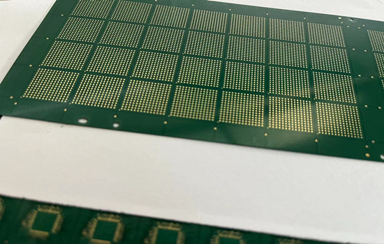
핀은 보드의 격자 패턴으로 이동합니다.. PCB의 모든 집적 회로 간에 전기 신호를 전달합니다.. 기판에 보이는 작은 솔더 볼은 BGA입니다..
BGA는 표면 실장 기술의 일종인 볼 그리드 어레이(Ball Grid Array)에 불과합니다.( SMT ), 부품과 PCB 사이의 납땜을 의미합니다.. BGA는 1~100만 개의 멀티플렉서를 포함하는 많은 중첩 레이어로 구성됩니다., 논리 게이트, 플립플롭 또는 기타 회로. BGA는 PCB의 친숙한 구성 요소입니다., BGA 구성 요소는 다양한 모양과 크기를 포함하는 표준화된 패키지에 전자적으로 포장됩니다., 리드 수가 많은 것으로 유명합니다, 작은 인덕턴스와 고효율 밀도. BGA의 적용이 PCB 제조에 중요한 역할을 한다는 것은 의심의 여지가 없습니다..
BGA 패키지 유형
다양한 기판을 기반으로 다음과 같이 주로 세 가지 BGA 유형이 있습니다.:
PBGA (플라스틱 볼 그리드 어레이)
CBGA (도자기 볼 그리드 어레이)
TBGA (테이프 볼 그리드 어레이)
PBGA ( 플라스틱 BGA ): BT 수지/유리 라미네이트를 기판으로 사용하는 다층 PCB, 플라스틱을 포장재로 사용. PBGA는 주로 저비용 요구를 충족하는 중~고효율 장치에 사용됩니다., 낮은 인덕턴스, 표면 장착이 용이하지만 패키징에 대한 높은 수준의 신뢰성. 게다가, PBGA는 전력 손실을 처리하기 위해 기판에 추가 구리 층을 가지고 있습니다..
TBGA (테이프 BGA ): 구멍이 있는 구조, 이는 열 발산 기능이 있지만 외부 방열판이 없는 애플리케이션에 적합한 솔루션입니다.. 칩과 기판 사이에는 두 가지 종류의 상호 연결이 있습니다.: 역 솔더 본딩 및 리드 본딩.
CBGA ( 도자기 BGA ): 다층 세라믹을 기판으로 사용합니다.. 금속 커버 PCB는 칩을 보호하기 위해 밀봉된 솔더로 기본 기판에 납땜됩니다., 리드와 패드.
질문이 있으시면, 저희에게 연락 주시기 바랍니다 info@alcantapcb.com , 기꺼이 도와드리겠습니다.