주식회사")
초박형 5G 기판 제조사. 첨단 초박형 5G로서 기판 제조업체, 차세대 고속통신을 위한 최첨단 기판을 전문적으로 생산하고 있습니다.. 당사의 초박형 기판은 탁월한 신호 무결성을 제공합니다., 강화 된 열 관리, 탁월한 신뢰성, 5G 기술의 엄격한 요구 사항 충족. 혁신과 품질에 중점을 두고, 우리는 고성능 장치에 힘을 실어주는 기판을 제공합니다, 빠르게 진화하는 5G 환경에서 원활한 연결과 최적의 성능 보장.
5G 기술의 출현은 통신에 혁명을 가져왔습니다., 유례없는 데이터 속도 약속, 매우 낮은 대기 시간, 대규모 연결성. 이러한 까다로운 요구 사항을 충족하려면, 5G 기기에 사용되는 기판은 고도로 발전해야 합니다. 초박형 5G 기판은 이러한 최첨단 애플리케이션을 지원하도록 설계되었습니다., 고성능 제공, 뛰어난 신호 무결성, 컴팩트한 폼 팩터로 효율적인 열 관리. 이 기사에서는 기능을 살펴봅니다., 디자인 고려 사항, 재료, 제조 공정, 애플리케이션, 초박형 5G 기판의 장점.
초박형 5G 기판이란??
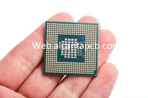
초박형 5G 기판은 인쇄회로기판의 일종이다. (PCB) 5G 기술의 고주파수 및 고속 요구 사항을 지원하도록 특별히 설계된 소재. 이 기판은 최소 두께가 특징입니다., 높은 열전도율, 그리고 우수한 전기적 특성, 5G 장치 및 인프라 통합에 이상적입니다.. 초박형 프로파일로 작고 가벼운 디자인이 가능합니다., 이는 현대 통신 장치에 매우 중요합니다..
초박형 5G 기판 특성
초박형 5G 기판은 고성능 애플리케이션에 적합한 몇 가지 주요 특성을 가지고 있습니다.:
이 기판은 5G 신호와 관련된 고주파수를 처리하도록 설계되었습니다., 최소한의 신호 손실과 우수한 전송 품질 보장.
효과적인 열 전도성은 고속 전자 부품에서 발생하는 열을 방출하는 데 중요합니다., 안정적인 작동 온도 유지 및 과열 방지.
초박형 프로파일은 어느 정도의 유연성을 제공합니다., 이는 성능 저하 없이 기판을 구부리거나 구부려야 하는 응용 분야에 유용합니다..
얇음에도 불구하고, 이 기판은 치수 안정성을 유지합니다., 제조 및 작동 중에 구성 요소의 정확한 정렬 및 배치 보장.
고순도 소재 사용으로 불량 및 불순물 최소화, 5G 기기의 성능에 영향을 줄 수 있는.
초박형 5G 기판 설계 고려 사항
초박형 5G 기판을 설계하려면 최적의 성능과 신뢰성을 보장하기 위해 몇 가지 중요한 고려 사항이 필요합니다.:
기판 재료의 선택이 중요합니다. 액정 폴리머와 같은 재료 (LCP), 폴리테트라플루오로에틸렌 (PTFE), 및 기타 고성능 폴리머는 우수한 전기적 및 열적 특성으로 인해 일반적으로 사용됩니다..
과열을 방지하려면 효율적인 열 관리가 필수적입니다.. 설계에는 열 방출에 대한 조항이 포함되어야 합니다., 열 비아 및 열 확산기 등.
고주파수에서 신호 무결성을 유지하는 것이 중요합니다.. 여기에는 트레이스 임피던스의 정밀한 제어가 포함됩니다., 신호 간섭 최소화, 효과적인 차폐 기술을 구현합니다.
기판은 제조 공정 및 작동 조건의 스트레스를 견딜 수 있도록 적절한 기계적 강도와 유연성을 가져야 합니다..
성분의 적절한 접착력과 정렬을 보장하기 위해 표면 마감은 매끄럽고 결함이 없어야합니다..
초박형 5G 기판에 사용되는 재료
초박형 5G 기판 제조에는 여러 가지 재료가 일반적으로 사용됩니다.:
LCP는 우수한 전기적 특성으로 알려져 있습니다., 높은 열 안정성, 그리고 흡습성이 낮다, 고주파 응용 프로그램에 이상적입니다.
PTFE는 우수한 전기 절연성과 내열성을 제공합니다., RF 및 마이크로웨이브 애플리케이션에 널리 사용되는 선택입니다..
폴리이미드 기판은 탁월한 열 안정성과 기계적 유연성을 제공합니다., 굽힘이나 굴곡이 필요한 용도에 적합.
고급 세라믹 소재, 알루미나, 질화알루미늄 등, 높은 열 전도성과 우수한 전기 절연성을 제공합니다., 고전력 애플리케이션에 적합하게 만듭니다..
유리 기판은 투명성과 절연성을 위해 사용됩니다., 특히 광전자 장치에서.
초박형 5G 기판 제조 공정
초박형 5G 기판의 제조 공정에는 고품질과 성능을 보장하기 위한 몇 가지 정밀한 단계가 포함됩니다.:
재료를 준비하고 크기에 맞게 잘라줍니다. 폴리머 기판용, 여기에는 재료를 얇은 시트로 압출하거나 주조하는 작업이 포함됩니다..
원하는 두께와 특성을 얻기 위해 여러 층의 기판 재료를 함께 적층할 수 있습니다.. 이 과정에는 층을 접착하기 위해 열과 압력이 필요합니다..
회로 패턴은 포토 리소그래피 프로세스를 사용하여 생성됩니다. 감광성 필름 (포토 레지스트) 기판에 적용됩니다, 자외선에 노출됩니다 (UV) 마스크를 통해 빛, 원하는 회로 패턴을 나타 내기 위해 개발되었습니다. 이어서, 기판을 에칭하여 원치 않는 재료를 제거한다.
VIAS는 기판으로 뚫어 서로 다른 층간에 수직 전기 연결을 생성합니다.. 그런 다음이 구멍은 구리로 도금되어 전도성 경로를 설정합니다..
무전해 니켈 침지 금과 같은 표면 마감재 (동의하다) 또는 납땜성을 향상시키고 산화를 방지하기 위해 접촉 패드에 침지 은을 적용합니다..
최종 기판은 조립을 거칩니다., 구성 요소가 추가되는 곳. 엄격한 테스트, 신호 무결성 테스트 포함, 임피던스 매칭 테스트, 및 환경 스트레스 테스트, 기판이 성능 표준을 충족하는지 확인하기 위해 수행됩니다..
초박형 5G 기판의 응용
초박형 5G 기판은 다양한 고성능 애플리케이션에 사용됩니다.:
이러한 기판은 고밀도 제조에 필수적입니다., 최신 스마트폰과 태블릿에 사용되는 고성능 PCB, 더 빠른 데이터 속도와 향상된 연결성 제공.
초박형 기판은 안정적인 신호 전송 및 수신에 필요한 고주파 RF 구성 요소를 지원하기 위해 5G 기지국에 사용됩니다..
초박형 기판의 유연성과 소형화로 인해 웨어러블 장치에 이상적, 가볍고 내구성이 뛰어난 전자 부품이 필요한 제품.
자동차 산업에서, 이 기판은 고급 운전자 지원 시스템에 사용됩니다 (ADAS) 기타 고성능 전자 시스템.
초박형 기판은 고속 처리와 안정적인 성능이 요구되는 의료 기기에 사용됩니다., 진단 영상 시스템, 첨단 모니터링 장비 등.
초박형 5G 기판의 장점
초박형 5G 기판은 고성능 애플리케이션에 없어서는 안 될 여러 가지 장점을 제공합니다.:
이 기판은 5G 신호와 관련된 고주파수를 처리하도록 설계되었습니다., 최소한의 신호 손실과 우수한 전송 품질 보장.
레이어드 디자인으로 효율적인 열 방출이 가능합니다., 과열 방지 및 안정적인 작동 보장.
초박형 프로파일은 어느 정도의 유연성을 제공합니다., 성능 저하 없이 굽힘이나 굴곡이 필요한 응용 분야에 유용합니다..
이러한 기판의 두께가 줄어들어 더욱 작고 가벼운 디자인이 가능해졌습니다., 이는 현대 통신 장치에 매우 중요합니다..
고순도 소재 사용으로 불량 및 불순물 최소화, 5G 기기의 안정적인 성능 보장.
FAQ
초박형 5G 기판 사용의 주요 이점은 무엇입니까??
주요 이점은 고주파 성능을 포함합니다., 효율적인 열 관리, 기계적 유연성, 컴팩트하고 가벼운 디자인, 그리고 고순도 소재를 사용하여, 고속 애플리케이션에서 안정적인 성능 보장.
초박형 5G 기판 제조에 일반적으로 사용되는 재료는 무엇입니까??
일반적인 재료에는 액정 폴리머가 포함됩니다. (LCP), 폴리테트라플루오로에틸렌 (PTFE), 폴리이미드, 고급 도자기, 그리고 유리. 이 재료는 우수한 전기 및 열 특성을 위해 선택됩니다..
초박형 5G 기판 설계는 어떻게 신호 무결성을 보장합니까??
제어된 임피던스를 제공하여 신호 무결성을 보장하는 설계, 신호 간섭 최소화, 효과적인 차폐 기술을 구현합니다. 시뮬레이션 도구는 고주파 성능을 위해 이러한 측면을 최적화하는 데 사용됩니다..
초박형 5G 기판의 일반적인 응용 분야는 무엇입니까??
일반적인 애플리케이션에는 스마트폰과 태블릿이 포함됩니다., 5G 기지국, 웨어러블 기기, 자동차 전자, 의료기기. 이 기판은 고밀도 상호 연결이 필요한 시스템 및 신뢰할 수있는 성능이 필요한 시스템에 사용됩니다..