CO., LTD")
Ultrathin IC Sehemu ndogo za kifurushi Manufacturer.We are a leading manufacturer of ultrathin IC package substrates, kutoa suluhisho za kisasa kwa vifaa vya elektroniki vya utendaji wa juu. Mbinu zetu za juu za utengenezaji huhakikisha ubora wa kipekee, kuwezesha uboreshaji mdogo na utendakazi ulioimarishwa katika programu mbalimbali, kutoka simu mahiri hadi vifaa vya matibabu. Tuamini kwa ubunifu, ya kuaminika, and efficient IC package substrates that meet the demands of today’s technology-driven world.
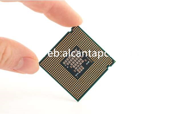
Ultrathin IC (Mzunguko Uliounganishwa) kifurushi substrates are a vital component in modern electronics, enabling the miniaturization and enhanced performance of various devices. These substrates are engineered to be extremely thin while maintaining the necessary electrical, mafuta, and mechanical properties to support high-performance ICs. Ultrathin substrates are particularly important in applications where space is at a premium, kama vile simu mahiri, vifaa vya kuvaa, na mifumo ya juu ya kompyuta.
What is an Ultrathin IC Package Substrate?
An ultrathin IC package substrate is a specialized type of printed circuit board (PCB) designed to provide a platform for mounting and interconnecting ICs. Substrates hizi zina sifa ya unene wao mdogo, kawaida chini ya 100 mikromita, which allows for the development of ultra-compact electronic packages. Licha ya wembamba wao, ultrathin substrates must support high-density interconnections, Usimamizi mzuri wa mafuta, and robust mechanical stability to ensure the reliable operation of the ICs they host.
Ultrathin IC Package Substrate Design Reference Guide
Designing ultrathin IC package substrates involves a comprehensive approach to ensure optimal performance and reliability.
The selection of materials is critical for achieving the desired properties in ultrathin substrates:
High-Density Polyimide Films: These materials offer excellent flexibility, utulivu wa juu wa joto, and good electrical insulation, making them ideal for ultrathin applications.
Foil za shaba: Used for conductive traces and interconnections, copper foils must be thin yet durable to maintain electrical performance without adding significant bulk.
Adhesives and Dielectrics: Advanced adhesives and dielectric materials with low dielectric constants and high thermal conductivity are used to bond the layers and provide insulation.
The layer structure of ultrathin substrates is designed to maximize space efficiency and performance:
Safu za Ishara: These layers are configured to minimize signal loss and crosstalk. Techniques such as microstrip and stripline are used to maintain controlled impedance.
Nguvu na Tabaka za Ardhi: Dedicated power and ground planes are crucial for stable power distribution and noise reduction, ensuring reliable IC operation.
Tabaka za Usimamizi wa Joto: Integrating thermal vias and heat spreaders helps to dissipate heat effectively, kuzuia overheating ya vipengele muhimu.
Interconnect Layers: High-density interconnects (HDI) with microvias and through-holes enable complex routing within the constrained space of ultrathin substrates.
What Materials are Used in Ultrathin IC Package Substrates?
Materials used in ultrathin IC package substrates are selected for their ability to meet stringent performance requirements:
High-Density Polyimide Films: Offering excellent flexibility, utulivu wa mafuta, na insulation ya umeme, these films are a common choice for ultrathin applications.
Foil za shaba: Thin yet durable copper foils are used for conductive traces and interconnections, ensuring reliable electrical performance.
Adhesives and Dielectrics: Advanced adhesives and dielectric materials with low dielectric constants and high thermal conductivity are used to bond the layers and provide insulation.
Reinforced Epoxy Resins: These materials enhance the mechanical strength of the substrate while maintaining a low profile.
What Size are Ultrathin IC Package Substrates?
The size of ultrathin IC package substrates varies depending on the specific application and device requirements:
Unene: Ultrathin substrates are typically less than 100 micrometers nene, with some designs reaching even lower thicknesses to accommodate the smallest form factors.
Urefu na Upana: These dimensions are determined by the size of the IC and the layout of the interconnections. Ukubwa wa kawaida huanzia milimita chache kwa IC ndogo hadi sentimita kadhaa kwa vifurushi vikubwa..
The Manufacturing Process of Ultrathin IC Package Substrates
The manufacturing process for ultrathin IC package substrates involves several precise and controlled steps to ensure high quality and performance:
High-density polyimide films, vifaa vya conductive, na adhesives ni tayari na kukatwa katika ukubwa sahihi kwa ajili ya usindikaji.
Safu zinatengenezwa na laminating vifaa vya conductive na kuhami katika stack. Kila safu ina muundo kwa kutumia upigaji picha ili kufafanua mzunguko.
Microvias na kupitia-mashimo hupigwa kwa kutumia mbinu za laser au mitambo ya kuchimba visima. Mashimo haya huwekwa kwa shaba ili kuunda miunganisho ya umeme kati ya tabaka.
Michakato ya upigaji picha na uandishi hutumiwa kuunda mzunguko wa sauti laini kwenye kila safu. Hatua hii inahitaji usahihi wa juu ili kuhakikisha miunganisho sahihi na ya kuaminika.
Baada ya kutengeneza safu, tabaka ni laminated pamoja chini ya joto na shinikizo. Substrate iliyokusanyika hupitia majaribio makali, ikiwa ni pamoja na kupima umeme, Baiskeli ya mafuta, na vipimo vya mkazo wa mitambo, ili kuhakikisha utendaji na uaminifu.
The Application Area of Ultrathin IC Package Substrates
Ultrathin IC package substrates enable advanced capabilities in a wide range of applications:
Katika simu mahiri, vidonge, na vifaa vinavyoweza kuvaliwa, ultrathin substrates support the compact and efficient integration of advanced ICs, enhancing performance and functionality while reducing size and weight.
Katika seva, Vituo vya data, na kompyuta kubwa, ultrathin substrates enable the integration of powerful processors and memory modules in a compact form factor, facilitating fast data processing and storage.
Sehemu ndogo hizi ni muhimu katika miundombinu ya mawasiliano ya simu, ikiwa ni pamoja na vituo vya msingi na vifaa vya mtandao, providing reliable and high-speed connectivity in a compact footprint.
In various consumer electronics, from smart home devices to gaming consoles, ultrathin substrates enable high performance in sleek, space-efficient designs.
Katika picha za matibabu na vifaa vya uchunguzi, ultrathin substrates support high-speed data acquisition and processing, kuboresha usahihi na ufanisi katika taratibu za matibabu.
What are the Advantages of Ultrathin IC Package Substrates?
Ultrathin IC package substrates offer several advantages that make them indispensable for advanced electronic applications:
Ubunifu wa Kompakt: The ultra-thin profile allows for the miniaturization of electronic packages, enabling more compact and portable devices.
Utendaji wa Juu: Nyenzo na muundo ulioboreshwa huhakikisha uadilifu wa juu wa ishara, hasara ya chini ya nguvu, na usimamizi bora wa joto.
Kuegemea Kuimarishwa: Michakato ya juu ya utengenezaji na nyenzo hutoa kuegemea juu, kuhakikisha utendaji wa muda mrefu katika mazingira yenye mahitaji.
Kubadilika: The thin and flexible nature of these substrates makes them suitable for a wide range of applications, from rigid high-performance devices to flexible and wearable electronics.
Scalability: Ultrathin substrates can be customized to meet the specific needs of various applications, kutoka kwa vifaa vidogo vya watumiaji hadi mifumo mikubwa ya viwanda.
Maswali
What are the key considerations in designing ultrathin IC package substrates?
Mambo muhimu ya kuzingatia ni pamoja na uteuzi wa nyenzo kwa mali ya umeme na ya joto, uboreshaji wa muundo wa safu kwa uadilifu wa ishara na usimamizi wa joto, na kuhakikisha utulivu wa mitambo na kuegemea.
How do ultrathin IC package substrates differ from standard PCBs?
Ultrathin IC package substrates are significantly thinner, with more layers and higher interconnect density, designed to handle higher frequencies and power levels compared to standard PCBs, kuwafanya kufaa kwa maombi ya juu.
What is the typical manufacturing process for ultrathin IC package substrates?
Mchakato unahusisha maandalizi ya nyenzo, utengenezaji wa safu, kuchimba visima na plating, muundo wa mzunguko, mkutano, na upimaji mkali ili kuhakikisha utendaji wa hali ya juu na kuegemea.
What are the main applications of ultrathin IC package substrates?
These substrates are used in mobile devices, Kompyuta ya utendaji wa juu, mawasiliano ya simu, Elektroniki za Watumiaji, na vifaa vya matibabu, kutoa utendakazi wa hali ya juu na kutegemewa katika nyanja hizi.