CO., LTD")
Mtengenezaji wa Sehemu ndogo ya IC ya Ultrathin.”Ultrathin Sehemu ndogo ya IC Mtengenezaji” mtaalamu wa kutengeneza substrates nyembamba na zenye utendakazi wa hali ya juu kwa saketi zilizounganishwa (ICs). Michakato yetu ya juu ya utengenezaji inahakikisha usahihi na kutegemewa, kukidhi mahitaji ya maombi ya kisasa ya kielektroniki.
Ultrathin IC Substrate ni nini?
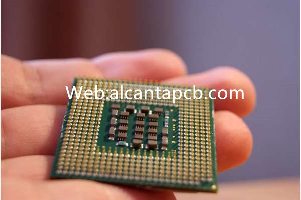
Sehemu ndogo za IC nyembamba sana ni laha bapa nyembamba sana zinazotumiwa kupachika na kuunganisha vijenzi vya kielektroniki. Sehemu ndogo hizi hufikia muunganisho kati ya vijenzi vya kielektroniki kwa kupachika nyaya za shaba zinazopitisha, pedi na vipengele vingine kwenye vifaa vya kuhami joto. Ikilinganishwa na bodi za mzunguko wa jadi zilizochapishwa (PCBs), Sehemu ndogo za IC nyembamba sana zina punguzo kubwa la unene na zinafaa kwa programu zilizo na nafasi ya juu na mahitaji ya uzito..
Katika muundo wa kisasa wa bidhaa za elektroniki, IC nyembamba sana substrates zinazidi kutumika. Pamoja na kuendelea kwa miniaturization na mseto wa kazi za vifaa vya elektroniki, ukubwa na mahitaji ya utendaji wa substrates yanazidi kuwa magumu zaidi. Kuibuka kwa substrates za IC nyembamba sana hukidhi mahitaji haya kwa usahihi. Tabia zake nyembamba sana sio tu kuokoa nafasi, lakini pia kupunguza sana uzito wa vifaa. Hii ni muhimu sana kwa bidhaa za kielektroniki zinazobebeka kama vile simu mahiri, vidonge, na vifaa vinavyoweza kuvaliwa. Kwa kupunguza unene, Sehemu ndogo za IC nyembamba sana zinaweza kufanya vifaa hivi kuwa vyepesi na kubebeka zaidi, huku pia ikiboresha uzuri wa jumla wa kifaa.
Sehemu ndogo za IC nyembamba sana hutengenezwa kwa nyenzo za utendaji wa juu kama vile polyimide au polima kioevu kioo. (LCP). Vifaa hivi vina mali bora ya insulation ya umeme na nguvu za mitambo, kuhakikisha utendaji wa kuaminika hata wakati substrate ni nyembamba sana. Aloi za shaba au shaba kawaida hutumiwa kama tabaka za conductive ili kuhakikisha upitishaji thabiti na wa kuaminika wa ishara za umeme.. Mchakato wa kutengeneza substrates za IC nyembamba zaidi ni ngumu sana na zinahitaji michakato na vifaa sahihi. Kwanza, filamu nyembamba sana ya shaba huwekwa kwenye nyenzo ndogo kupitia uwekaji wa kemikali au uwekaji wa mvuke halisi. Basi, teknolojia ya photolithografia hutumiwa kuunda muundo wa mzunguko unaohitajika kwenye filamu ya shaba, na kisha shaba iliyozidi huondolewa kupitia mchakato wa etching, kuacha tu muundo wa mzunguko unaohitajika.
Sehemu ndogo za IC nyembamba sana hazitumiwi tu katika bidhaa za kielektroniki za watumiaji, lakini pia ina jukumu muhimu katika nyanja zinazohitajika sana kama vile vifaa vya matibabu, Anga, na umeme wa magari. Katika maeneo haya, kubebeka kwa kifaa na utendakazi wa hali ya juu ni muhimu, na substrates za IC nyembamba sana ni bora kwa kukidhi mahitaji haya.
Kwa jumla, kuibuka kwa substrates za IC nyembamba zaidi inawakilisha maendeleo muhimu katika teknolojia ya utengenezaji wa kielektroniki. Sio tu inakidhi mahitaji ya vifaa vya kisasa vya umeme kwa miniaturization, kubebeka na utendaji wa juu, lakini pia inakuza uvumbuzi na maendeleo katika muundo wa bidhaa za kielektroniki. Pamoja na maendeleo endelevu ya teknolojia na upanuzi unaoendelea wa matumizi, IC substrates nyembamba sana zitachukua jukumu muhimu zaidi katika ulimwengu wa kielektroniki wa siku zijazo.
Mwongozo wa Marejeleo wa Usanifu wa Kidogo cha IC cha Ultrathin.
Wakati vifaa vya elektroniki vinakua kuwa nyembamba, nyepesi na utendaji wa juu, Sehemu ndogo za IC nyembamba sana zimekuwa lengo la tasnia. Mwongozo wa Marejeleo ya Muundo wa Kitengo Ndogo cha Ultra-Thin IC ni mwongozo wa kina ulioandikwa kwa ajili ya wahandisi na wabunifu ili kuwasaidia kuunda muundo bora na wa kuaminika wa substrate ya IC.. Mwongozo unashughulikia mazoea bora, sheria za kubuni, zana za programu na teknolojia zinazohusiana ili kuhakikisha miundo inakidhi mahitaji magumu ya vifaa vya kisasa vya kielektroniki.
Wakati wa kuunda substrates za IC nyembamba zaidi, ni muhimu kufuata mazoea bora. Kwanza, kufafanua malengo ya kubuni na mahitaji ya kazi, na uchague nyenzo zinazofaa na idadi ya tabaka kulingana na programu maalum. Pili, boresha mpangilio na uelekezaji ili kuhakikisha uadilifu wa ishara na utendaji wa umeme. Hatimaye, muundo wa usimamizi wa mafuta unafanywa ili kuzuia overheating kutoka kwa vipengele vya kuharibu na kuboresha utulivu wa mfumo.
Sheria za muundo ndio msingi wa kuhakikisha utendakazi wa kutegemewa kwa substrates za IC nyembamba sana. Wakati wa mchakato wa kubuni, sheria za msingi zifuatazo zinapaswa kufuatwa: 1) Upana wa chini wa mstari na nafasi ya mstari lazima utimize mahitaji ya mchakato wa utengenezaji ili kuzuia saketi fupi na kuingiliwa kwa mawimbi; 2) Panga vipengele ipasavyo ili kuhakikisha usambazaji sawa wa nyaya za nguvu na ardhi na kupunguza kuingiliwa kwa sumakuumeme; 3) Fikiria nguvu za mitambo na upanuzi wa joto ili kuepuka kuinama na kupasuka kwa substrate.
Muundo wa kisasa hauwezi kutenganishwa na zana za programu za hali ya juu. Programu ya kubuni inayotumiwa kawaida ni pamoja na Cadence Allegro, Mbuni wa hali ya juu, Picha za Mentor, nk. Zana hizi hutoa uwekaji na utendakazi wa kuelekeza, uchanganuzi wa uadilifu wa ishara na uwezo wa uigaji wa halijoto ili kusaidia wabunifu kuboresha miundo haraka na kuthibitisha uwezekano wao.. Aidha, kutumia zana za uundaji otomatiki (EDA) inaweza kuboresha ufanisi wa muundo na kupunguza makosa ya kibinadamu.
Mbali na sheria za kubuni na zana za programu, kusimamia teknolojia zinazohusiana ni muhimu vile vile. Kwanza, kuelewa teknolojia ya microwave na masafa ya redio ili kukabiliana na mahitaji ya upitishaji wa mawimbi ya masafa ya juu. Pili, bwana teknolojia ya kubuni bodi ya safu nyingi na kutambua ujumuishaji wa mizunguko tata. Hatimaye, kuwa na ufahamu na mbinu za ufungaji na mkusanyiko ili kuhakikisha uunganisho wa kuaminika wa vipengele.
Muundo wa sehemu ndogo ya IC nyembamba sana ni kazi ngumu na tete, inayohitaji wabunifu kuwa na ujuzi na uzoefu wa kina. Kwa kufuata mazoea bora, sheria za kubuni, na kutumia zana za programu za hali ya juu na teknolojia zinazohusiana, wahandisi na wabunifu wanaweza kuunda substrates za IC zenye ufanisi na za kuaminika, kutoa msingi imara kwa ajili ya maendeleo ya vifaa vya kisasa vya kielektroniki.
Madhumuni ya mwongozo huu ni kusaidia wabunifu kuelewa kwa utaratibu na kusimamia vipengele vyote vya muundo wa IC nyembamba sana., hivyo kuboresha ufanisi wa muundo na ubora wa bidhaa, na kutoa msaada mkubwa kwa uvumbuzi wa kiteknolojia.
Ni nyenzo gani inatumika kwenye Kidogo cha Ultrathin IC?
Sehemu ndogo za IC nyembamba sana ni muhimu sana na ni sehemu muhimu katika vifaa vya kisasa vya kielektroniki, na utendaji wao na uaminifu kwa kiasi kikubwa hutegemea mali ya vifaa vinavyotumiwa. Kawaida, Sehemu ndogo za IC nyembamba sana zimetengenezwa kwa nyenzo zenye utendaji wa juu ili kukidhi mahitaji magumu katika suala la insulation ya umeme., nguvu ya mitambo, na conductivity.
Kwanza kabisa, nyenzo za msingi za substrates za IC nyembamba sana mara nyingi ni polyimide (Polyimide) au polymer ya kioo kioevu (LCP). Nyenzo hizi mbili ni maarufu katika sekta ya umeme hasa kutokana na mali zao bora. Polyimide ni polima iliyo na uimara wa hali ya juu wa mafuta ambayo hudumisha nguvu zake za mitambo na sifa za insulation za umeme hata katika mazingira ya joto la juu.. Hii inafanya polyimide kuwa nyenzo bora kwa matumizi katika hali ngumu ya kufanya kazi. Polima za kioo za kioevu zinajulikana kwa mgawo wao wa chini wa upanuzi wa joto na upinzani wa juu wa kemikali, kuzifanya kuwa bora katika programu zinazohitaji usahihi wa hali ya juu na uimara.
Mbali na nyenzo za msingi, IC substrates nyembamba sana pia ni pamoja na safu ya chuma conductive, kawaida aloi za shaba au shaba. Hii ni kwa sababu shaba ina conductivity bora ya umeme na inaweza kusambaza ishara za umeme kwa ufanisi. Aidha, unyumbulifu wa mitambo ya shaba na uchakataji pia huifanya kuwa bora kwa kutengeneza mifumo changamano ya saketi. Katika baadhi ya maombi yanayohitaji, aloi za shaba zinaweza kuchaguliwa ili kuongeza zaidi nguvu ya mitambo ya nyenzo na uimara.
Ili kutengeneza substrates za IC nyembamba sana, nyenzo hizi lazima zipitie mfululizo wa taratibu za maridadi. Kwanza, substrate ya polyimide au kioo kioevu ya polima imeandaliwa kwenye karatasi nyembamba inayohitajika, na kisha safu sare ya aloi ya shaba au shaba inawekwa juu ya uso wake kupitia uwekaji wa kemikali au mchakato wa uwekaji wa umeme.. Inayofuata, mifumo sahihi ya mzunguko huundwa kwenye safu ya shaba kwa njia ya photolithography na taratibu za etching. Hatimaye, baada ya kuchimba visima na hatua za soldering, mkusanyiko wa substrate na uhusiano wa umeme umekamilika.
Uteuzi wa nyenzo hizi na michakato ya utengenezaji wa substrates za IC nyembamba zaidi sio tu kuhakikisha utendaji wake wa juu na kutegemewa., lakini pia huiwezesha kukidhi mahitaji ya miniaturization na ushirikiano wa hali ya juu wa vifaa vya kisasa vya kielektroniki. Iwe katika utendakazi wa juu wa kompyuta, Smartphones, vifaa vya kuvaliwa au nyanja zingine za hali ya juu, Sehemu ndogo za IC nyembamba sana zimekuwa na jukumu lisiloweza kubadilishwa na muhimu.
Kwa kifupi, nyenzo kuu za substrates za IC nyembamba zaidi ni pamoja na polyimide na polima kioevu kioo kama nyenzo ya msingi., na aloi ya shaba au shaba kama safu ya conductive. Uteuzi na mchanganyiko wa nyenzo hizi hutoa substrates za IC nyembamba zaidi mali bora za insulation za umeme, nguvu ya mitambo na conductivity, kuwaruhusu kuchukua jukumu muhimu katika teknolojia ya kisasa ya kielektroniki.
Sehemu ndogo ya Ultrathin IC ni ya ukubwa gani?
Vipimo vya substrates za IC nyembamba sana hutofautiana kulingana na programu mahususi, kuzifanya zitumike sana katika vifaa vya kisasa vya kielektroniki. Pamoja na maendeleo ya sayansi na teknolojia na uboreshaji unaoendelea wa bidhaa za kielektroniki, mahitaji ya substrates ultra-thin IC imekuwa tofauti zaidi na zaidi. Kuanzia simu mahiri na vifaa vinavyoweza kuvaliwa hadi vifaa vya viwandani na bidhaa za kielektroniki za nguvu, ultra-thin IC substrates hutumiwa katika vifaa mbalimbali ina jukumu muhimu katika zote mbili.
Kwa simu mahiri na vifaa vinavyoweza kuvaliwa, vifaa hivi mara nyingi huhitaji ukubwa mdogo, uzito mwepesi, na nafasi ndogo sana ya ndani. Kwa hiyo, substrates za IC nyembamba sana lazima ziwe ndogo na nyembamba iwezekanavyo ili kukidhi mahitaji haya. Substrates vile kawaida ni ndogo kwa ukubwa, na unene ndani ya mikroni mia chache. Ukubwa mdogo na asili nyembamba sana ya substrates hizi huziruhusu kupachikwa kwa urahisi kwenye nafasi ngumu za vifaa huku zikidumisha utendakazi bora wa umeme na nguvu za mitambo.. Kwa mfano, sehemu ndogo ya IC nyembamba sana katika saa mahiri inaweza kuwa milimita chache tu za mraba, wakati unene unaweza kuwa kati 50 mikroni na 150 mikroni.
Kwa kulinganisha, vifaa vya viwandani na bidhaa za umeme zina mahitaji tofauti ya ukubwa wa substrate. Vifaa vile kawaida huhitaji kushughulikia nguvu za juu na nyaya ngumu zaidi, kwa hivyo saizi ya substrates za IC nyembamba sana ni kubwa kiasi cha kubeba vijenzi zaidi vya kielektroniki na nyaya changamano zaidi.. Ukubwa wa substrates hizi zinaweza kufikia sentimita kadhaa au hata makumi ya sentimita, na ingawa bado wanadumisha sifa nyembamba sana, unene ni mkubwa kidogo kuliko ule wa umeme wa watumiaji ili kuhakikisha nguvu za kutosha za mitambo na uwezo wa kusambaza joto.
Aidha, huku bidhaa za kielektroniki zikiendelea kupunguzwa na kuunganishwa, kunyumbulika kwa ukubwa na umbo la substrates za IC nyembamba sana imekuwa muhimu sana. Baadhi ya matukio ya juu ya programu, kama vile skrini zinazonyumbulika na bodi za saketi zenye safu nyingi zenye msongamano mkubwa, zinahitaji substrates na uhuru wa juu wa kubuni. Hii ina maana kwamba pamoja na substrates za jadi za mstatili na mraba, Sehemu ndogo za IC nyembamba sana zinaweza pia kuundwa katika maumbo na ukubwa mbalimbali changamano kulingana na mahitaji maalum ili kukabiliana na miundo ya ndani ya vifaa mbalimbali..
Kwa kifupi, ukubwa wa substrates ultra-thin IC ni kuamua kulingana na mahitaji ya maombi maalum. Kuanzia simu mahiri na vifaa vidogo vinavyoweza kuvaliwa hadi vifaa vikubwa vya viwandani na sehemu ndogo za umeme, kila programu ina mahitaji yake maalum ya ukubwa na unene. Unyumbulifu huu wa kipenyo hufanya sehemu ndogo za IC nyembamba sana kuwa sehemu ya lazima ya vifaa vya kisasa vya kielektroniki.. Sio tu inakidhi mahitaji tofauti ya muundo, lakini pia kukuza miniaturization, nyepesi na utendaji wa juu wa bidhaa za elektroniki. kuendeleza.
Mchakato wa Mtengenezaji wa Ultrathin IC Substrate.
Mchakato wa utengenezaji wa substrates za IC nyembamba zaidi ni mchakato sahihi sana na wa hatua nyingi, na kila hatua inahitaji udhibiti mkali na uendeshaji wa usahihi wa juu ili kuhakikisha ubora na utendaji wa bidhaa ya mwisho. Zifuatazo ni hatua kuu katika utengenezaji wa mkatetaka mwembamba wa IC:
Hatua ya kwanza katika utengenezaji wa substrates za IC nyembamba zaidi ni kuandaa nyenzo za substrate. Nyenzo za substrate zinazotumiwa kawaida ni pamoja na polyimide (Polyimide) au polymer ya kioo kioevu (LCP), ambayo ina mali bora ya insulation ya umeme na nguvu za mitambo. Nyenzo za substrate kawaida hutolewa katika fomu ya filamu, ambayo hukatwa na kusafishwa ili kuhakikisha uso usio na vumbi.
Baada ya nyenzo za substrate kutayarishwa, safu ya shaba inahitaji kuwekwa kwenye uso wake. Hii kawaida hupatikana kwa uwekaji wa mvuke wa kemikali (CVD) au uwekaji wa mvuke halisi (PVD). Utaratibu huu unahitaji udhibiti kamili wa unene wa safu ya shaba ili kuhakikisha kuwa inatoa upitishaji mzuri wa umeme wakati wa kudumisha asili ya jumla ya nyembamba..
Hatua inayofuata ni mipako ya photoresist na mfiduo. Safu ya photoresist imewekwa kwenye substrate, na kisha muundo wa mzunguko ulioundwa unakadiriwa kwenye mpiga picha kupitia kinyago. Baada kuwepo hatarini, photoresist hupitia mabadiliko ya kemikali katika maeneo yaliyopigwa na mwanga.
Baada ya mfiduo na mchakato wa maendeleo, muundo wa shaba tu ambao unahitaji kubakishwa utaachwa kwenye substrate. Inayofuata, safu ya shaba isiyofunikwa na photoresist inaondolewa kupitia mchakato wa etching. Njia za kawaida za etching ni pamoja na etching mvua na etching kavu. Njia gani ya kuchagua inategemea mahitaji maalum ya kubuni na hali ya mchakato.
Baada ya etching kukamilika, mashimo yanahitaji kuchimbwa kwenye substrate kwa viunganisho vya umeme vinavyofuata. Mashimo haya yanaweza kupitia mashimo ya teknolojia ya kuweka mashimo (THT) au vipofu au kuzikwa kwa njia ya teknolojia ya mlima wa uso (Smt). Uchimbaji kwa kawaida hutumia vifaa vya kuchimba visima vya laser vya usahihi wa juu au vifaa vya kuchimba visima vya mitambo.
Baada ya kuchimba visima, vipengele vya elektroniki vinaanza kuwekwa kwenye substrate. Kwa mchakato wa SMT, vipengele vinawekwa moja kwa moja kwenye usafi kwenye uso wa substrate. Kwa mchakato wa THT, pini za sehemu huingizwa kwenye substrate kupitia mashimo yaliyochimbwa na kisha kuuzwa kwa upande mwingine wa substrate..
Baada ya vipengele vya elektroniki vimewekwa, hatua inayofuata ni soldering. Soldering inaweza kufanyika kwa reflow au wimbi soldering, kulingana na mbinu ya ufungaji inayotumiwa. Uuzaji wa reflow hutumiwa kwa vipengee vya SMT, wakati wimbi soldering ni kawaida kutumika kwa ajili ya vipengele THT.
Hatua ya mwisho ni kupima. Kupitia upimaji wa umeme na upimaji wa kazi, tunahakikisha kwamba kila sehemu ndogo ya IC nyembamba sana inakidhi vipimo vya muundo na mahitaji ya utendaji. Hatua za majaribio ni pamoja na utambuzi wa mzunguko wazi na mfupi, upimaji wa kazi na upimaji wa kuegemea ili kuhakikisha ubora wa juu na uaminifu wa bidhaa.
Mchakato wa utengenezaji wa substrates za IC nyembamba sana ni mchakato mgumu sana na sahihi unaohitaji utendakazi wa hatua nyingi na udhibiti mkali.. Kila hatua, kutoka kwa maandalizi ya substrate hadi majaribio ya mwisho, ni muhimu kwa ubora na utendaji wa bidhaa. Kwa kuboresha kila hatua ya utengenezaji, tunahakikisha kuwa sehemu ndogo ya mwisho ya IC nyembamba sana ina sifa bora za umeme na nguvu ya mitambo ili kukidhi mahitaji mbalimbali ya maombi..
Eneo la Utumizi la Ultrathin IC Substrate.
Sehemu ndogo za IC nyembamba sana huchukua nafasi muhimu katika teknolojia ya kisasa na hutumiwa sana katika tasnia nyingi., pamoja na umeme wa watumiaji, mawasiliano ya simu, Magari, Anga, Vifaa vya matibabu, na automatisering ya viwandani. Wasifu wao wa chini na utendakazi bora huwafanya kuwa vipengele muhimu katika vifaa na mifumo ya kielektroniki yenye utendaji wa juu.
Katika uwanja wa matumizi ya umeme, Sehemu ndogo za IC nyembamba sana hutumiwa sana katika bidhaa kama vile simu mahiri, vidonge, kompyuta za mkononi, na vifaa vinavyoweza kuvaliwa. Vifaa hivi vina mahitaji madhubuti ya nafasi na uzito, na uwezo wa kushikana na wiring wa msongamano wa juu wa substrates za IC nyembamba zaidi zinaweza kukidhi mahitaji haya.. Aidha, Sehemu ndogo za IC nyembamba zaidi zinaweza kuboresha utendakazi wa utaftaji wa joto wa vifaa na kupanua maisha ya huduma ya bidhaa za elektroniki..
Sekta ya mawasiliano ya simu pia inanufaika kutokana na manufaa ya sehemu ndogo za IC nyembamba sana. Vifaa vya kisasa vya mawasiliano, kama vile vituo vya msingi, ruta na vituo vya data, zinahitaji nguvu ya juu ya usindikaji na kasi ya uwasilishaji wa data haraka. Pamoja na utendaji wake bora wa umeme na sifa za juu-frequency, Sehemu ndogo za IC nyembamba zaidi zinaweza kusaidia upitishaji wa mawimbi ya kasi ya juu na kuhakikisha utendakazi thabiti na mawasiliano bora ya vifaa..
Katika tasnia ya magari, Sehemu ndogo za IC nyembamba sana hutumiwa katika vitengo mbalimbali vya udhibiti wa kielektroniki (Funika), sensorer na mifumo ya usimamizi wa betri ya magari ya umeme. Pamoja na uboreshaji unaoendelea wa umeme wa gari na akili, Sehemu ndogo za IC nyembamba zaidi husaidia kufikia miundo midogo na nyepesi, kuboresha utendaji wa jumla na ufanisi wa mafuta ya magari.
Sehemu ya anga ina mahitaji ya juu sana juu ya kuegemea na uimara wa vifaa vya elektroniki. Sehemu ndogo za IC nyembamba sana zina nguvu bora za kimitambo na uwezo wa kimazingira, na inaweza kudumisha utendaji thabiti chini ya hali mbaya. Zinatumika sana katika mifumo ya urambazaji, vifaa vya mawasiliano na mifumo ya udhibiti wa satelaiti, vyombo vya anga na ndege, kuhakikisha usalama na mafanikio ya misheni za anga.
Katika uwanja wa vifaa vya matibabu, Sehemu ndogo za IC nyembamba sana hutumiwa katika vifaa mbalimbali vya uchunguzi na matibabu, kama vile MRI, CT scanner na pacemakers. Vifaa hivi vinahitaji usahihi wa juu na kuegemea. Sehemu ndogo za IC nyembamba sana zinaweza kutoa upitishaji na udhibiti wa mawimbi sahihi ili kuhakikisha usahihi na kutegemewa kwa vifaa vya matibabu., hivyo kuboresha utambuzi na athari za matibabu.
Katika automatisering ya viwanda, Sehemu ndogo za IC nyembamba sana hutumiwa katika roboti za viwandani, mistari ya uzalishaji otomatiki na mifumo ya udhibiti. Wanawezesha ushirikiano wa juu-wiani wa nyaya tata, kusaidia usindikaji wa mawimbi ya kasi ya juu na udhibiti sahihi, na kuboresha ufanisi wa uzalishaji na ubora wa bidhaa.
Kwa kifupi, Sehemu ndogo za IC nyembamba sana zimekuwa sehemu kuu ya vifaa vya elektroniki katika tasnia anuwai kwa sababu ya faida zao za kipekee.. Wao sio tu kuboresha utendaji na uaminifu wa vifaa, lakini pia kukuza maendeleo na uvumbuzi wa teknolojia ya kielektroniki, kutoa msaada mkubwa kwa maisha ya kisasa na maendeleo ya viwanda.
Je, ni faida gani za Ultrathin IC Substrate?
Katika maendeleo ya vifaa vya kisasa vya elektroniki, IC substrates nyembamba sana hupendelewa kwa manufaa yake mengi. Ikilinganishwa na njia za jadi za wiring, Sehemu ndogo za IC nyembamba zaidi zina ubora katika ushikamano, kuegemea, urahisi wa mkusanyiko, ubinafsishaji na ufanisi wa gharama.
Kwanza, kushikana ni mojawapo ya faida muhimu za substrates za IC nyembamba sana. Kwa sababu ya asili yake nyembamba sana, Sehemu ndogo za IC nyembamba zaidi huruhusu mpangilio wa kushikana zaidi, ambayo ni muhimu sana kwa vifaa vya kielektroniki vinavyofuata uboreshaji mdogo. Smartphones, vifaa vya kuvaa, na vifaa vingine vya kielektroniki vinavyobebeka vyote vinanufaika kutokana na matumizi ya substrates za IC nyembamba sana, ambayo huwezesha utendaji zaidi kuunganishwa katika nafasi ndogo huku ikidumisha muundo mwembamba na mwepesi wa kifaa.
Pili, kuegemea ni faida nyingine kuu ya substrates za IC nyembamba sana. Sehemu ndogo za IC nyembamba sana hupitisha michakato ya utengenezaji iliyosanifiwa ili kuhakikisha uthabiti wa bidhaa na kutegemewa. Uthabiti huu sio tu kuboresha ubora wa bidhaa, pia hupunguza hatari ya kushindwa kutokana na tofauti za utengenezaji, na hivyo kuboresha utendaji wa jumla na maisha marefu ya kifaa cha kielektroniki.
Urahisi wa mkusanyiko ni faida ya tatu kuu ya substrates za IC nyembamba sana. Sehemu ndogo za IC nyembamba sana zinafaa kwa michakato ya kiotomatiki ya mkusanyiko, ambayo hurahisisha sana mchakato wa uzalishaji, inapunguza gharama za kazi, na kuboresha ufanisi wa uzalishaji. Mkutano wa kiotomatiki sio tu kuongeza kasi ya uzalishaji, lakini pia hupunguza makosa iwezekanavyo yanayosababishwa na uendeshaji wa mwongozo, zaidi kuhakikisha ubora wa bidhaa.
Aidha, ubinafsishaji huruhusu substrates za IC nyembamba sana kukidhi mahitaji mbalimbali mahususi. Ikiwa ni muundo mgumu wa mzunguko au ujumuishaji wa sehemu maalum, Sehemu ndogo za IC nyembamba sana zinaweza kutengenezwa na kutengenezwa kulingana na mahitaji maalum. Unyumbulifu huu huifanya kuwa bora katika matumizi mbalimbali, hasa katika vifaa vya elektroniki vya hali ya juu ambavyo vinahitaji ubinafsishaji wa hali ya juu.
Hatimaye, ufanisi wa gharama ni faida kubwa ya substrates za IC nyembamba zaidi katika uzalishaji wa wingi. Kupitia uzalishaji wa wingi, gharama ya kitengo cha substrates za IC nyembamba zaidi inaweza kupunguzwa, kuwafanya kuwa wa kiuchumi katika utengenezaji wa wingi. Hii bila shaka ni muhimu kuzingatia kwa wazalishaji wa vifaa vya elektroniki, kwani sio tu kwamba inapunguza gharama za uzalishaji bali pia inaboresha ushindani wa soko.
Kwa jumla, Sehemu ndogo za IC nyembamba sana zimekuwa sehemu muhimu katika utengenezaji wa vifaa vya kisasa vya kielektroniki kwa sababu ya kushikana kwao, kuegemea, urahisi wa mkusanyiko, ubinafsishaji, na ufanisi wa gharama. Na maendeleo endelevu ya sayansi na teknolojia, Sehemu ndogo za IC nyembamba zaidi zitatumika sana katika nyanja mbalimbali, kutoa msingi thabiti wa uvumbuzi na maendeleo ya vifaa vya elektroniki.
Maswali
Sehemu ndogo ya IC nyembamba sana ni nini?
Sehemu ndogo ya IC nyembamba sana ni sahani nyembamba sana ya gorofa inayotumiwa kuweka na kuunganisha vipengee vya kielektroniki. Uunganisho kati ya vipengele unapatikana kwa kuunganisha waya za shaba za conductive, pedi na vipengele vingine. Ikilinganishwa na PCB za jadi, Sehemu ndogo za IC nyembamba zaidi zimepunguzwa kwa unene na zinafaa kwa programu zilizo na nafasi ya juu na mahitaji ya uzito..
Ni nyenzo gani hutumika kwa substrates za IC nyembamba sana?
Sehemu ndogo za IC nyembamba sana hutengenezwa kwa nyenzo za utendaji wa juu kama vile polyimide na polima kioevu kioo. (LCP), ambayo hutoa mali bora ya insulation ya umeme na nguvu za mitambo. Aloi za shaba au shaba hutumiwa kwa safu ya chuma ili kuhakikisha conductivity nzuri na kuegemea.
Je, ni maeneo gani kuu ya utumiaji ya substrates za IC nyembamba sana?
Sehemu ndogo za IC nyembamba sana hutumiwa sana katika tasnia mbalimbali, pamoja na umeme wa watumiaji (kama vile simu mahiri na vifaa vinavyoweza kuvaliwa), mawasiliano ya simu (kama vile vifaa vya mawasiliano ya kasi ya juu), Magari (kama vile mifumo ya kielektroniki kwenye bodi), Anga (kama vile satelaiti na vyombo vya anga), Vifaa vya matibabu (kama vile vyombo vya uchunguzi vinavyobebeka) na automatisering ya viwandani (kama vile mifumo ya udhibiti wa usahihi).
Je! ni mchakato gani wa utengenezaji wa substrates za IC nyembamba sana?
Mchakato wa utengenezaji ni pamoja na utayarishaji wa substrate, utuaji wa safu ya shaba, mipako ya photoresist na mfiduo, etching, kuchimba visima, uwekaji wa sehemu, soldering na kupima. Teknolojia ya mlima wa uso (Smt) na teknolojia ya kuweka kwenye shimo (THT) hupitishwa kulingana na mahitaji ya muundo ili kuhakikisha uzalishaji bora na utendaji wa kuaminika.