CO., LTD")
Fabricante profissional de substrato ABF, Fornecedor de substratos FCBGA, Produzimos principalmente pitch ultra-pequeno com 4mil, traço e espaçamento ultrapequenos com 9um/9um, Fizemos os substratos do pacote FCBGA a partir de 4 camada para 20 camadas.
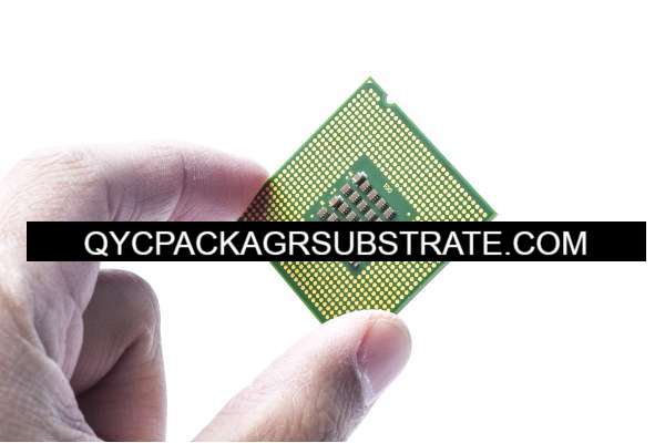
Substrato ABF, ou “Substrato de filme de construção Ajinomoto”, desempenha um papel vital em equipamentos eletrônicos modernos, especialmente na área de embalagens de circuitos integrados. Como um dos principais componentes do PCB engenharia, O Substrato ABF serve como base de todo o sistema eletrônico através de sua plataforma estável, fornecendo suporte confiável para conexões complexas em componentes eletrônicos.
Substrato ABF “ABF” vem de “Filme de construção da Ajinomoto”, que é um material de filme especial. Este material é amplamente utilizado na fabricação de dispositivos eletrônicos de alto desempenho, com embalagem de circuito integrado sendo uma de suas principais aplicações. Como engenheiro de PCB com dez anos de experiência, Conheço a importância do Substrato ABF na área de engenharia eletrônica.
O Substrato ABF não é apenas uma estrutura de suporte, mas também a pedra angular de conexões complexas entre componentes eletrônicos. Em embalagens de circuito integrado, O Substrato ABF fornece uma base estável para que componentes eletrônicos minúsculos e densos possam ser conectados de forma confiável em sua superfície. Isto não só melhora o desempenho dos equipamentos eletrônicos, mas também garante sua operação estável.
A tecnologia especial de membrana de construção deste substrato durante o processo de fabricação confere-lhe propriedades únicas. O projeto estrutural do Substrato ABF visa minimizar a distância entre os componentes eletrônicos, melhorando assim a eficiência da transmissão do sinal. Isto é particularmente importante nos dispositivos eletrônicos atuais que buscam alto desempenho e densidade.
De PWBs a placas-mãe, para substratos semelhantes (Fonoaudiólogos) e interconexão de alta densidade (HDI) substratos, O impacto do ABF Substrate está em toda parte. Comparado com PCB tradicional, O Substrato ABF não apenas fornece um maior grau de integração, mas também pode acomodar mais componentes eletrônicos em um espaço menor. Isso torna os dispositivos eletrônicos mais finos, isqueiro, e mais flexível sem sacrificar o desempenho.
Como engenheiro de PCB, Compreendo profundamente o valor do Substrato ABF na engenharia eletrônica. Não é apenas um material, mas também um dos principais fatores que promovem o progresso tecnológico dos equipamentos eletrónicos. Em um cenário tecnológico em evolução, um profundo conhecimento do Substrato ABF se tornará uma base importante para inovação e design futuros.
Quais são as funções do substrato ABF?
Na engenharia de PCB, O substrato ABF desempenha um papel fundamental na facilitação da operação perfeita do circuito integrado (Ic) embalagem com suas capacidades únicas. ABF, “Filme de construção da Ajinomoto”, O substrato é um componente indispensável dos equipamentos eletrônicos modernos. Sua principal função está focada em promover a interligação entre os diversos componentes do pacote de circuitos integrados..
A principal missão do ABF Substrate é servir como um meio de transmissão confiável, projetado para garantir uma transmissão suave de sinais e energia. Isso significa que em dispositivos eletrônicos, O Substrato ABF é responsável por transmitir e conectar sinais importantes para garantir a operação coordenada de todo o sistema. Seu design exclusivo permite que o ABF Substrate obtenha conexões eletrônicas complexas em um espaço minúsculo, fornecendo uma solução viável para o design compacto de dispositivos eletrônicos modernos.
Especificamente, O ABF Substrate permite que vários componentes do circuito integrado se comuniquem efetivamente entre si, fornecendo uma plataforma sólida e estável. Sua construção e seleção de materiais são projetadas para reduzir o ruído de transmissão de sinal, garantindo assim uma transmissão de sinal de alta qualidade. Esta natureza de interconexão cuidadosamente projetada é um dos fatores-chave para alcançar alto desempenho e confiabilidade em dispositivos eletrônicos modernos.
Como o núcleo dos dispositivos eletrônicos, outra função importante do ABF Substrate é garantir o funcionamento perfeito de dispositivos eletrônicos. Ao apoiar a comunicação eficiente entre componentes individuais, O Substrato ABF fornece uma base sólida para o desempenho geral do dispositivo. Ele não apenas transmite sinais, mas também assume a responsabilidade pela transmissão de energia, fornecendo uma solução confiável para consumo de energia do dispositivo e distribuição de energia.
Em geral, a função do Substrato ABF não se limita apenas a fornecer uma ponte de conexão, mas também a chave para garantir o bom funcionamento dos dispositivos eletrônicos. Seu papel nas embalagens de circuitos integrados vai muito além disso, fornecendo suporte sólido para o desenvolvimento e inovação da tecnologia eletrônica moderna. À medida que a tecnologia continua a avançar, podemos esperar que o Substrato ABF desempenhe um papel mais importante no futuro design eletrônico.
Quais são os diferentes tipos de substrato ABF?
Substrato ABF, um componente indispensável no campo da eletrônica, vem em muitos tipos, cada um personalizado para atender às necessidades específicas do crescente campo da eletrônica. Esses diferentes tipos de substrato ABF desempenham um papel fundamental no projeto de engenharia, fornecendo aos engenheiros e designers a oportunidade de otimizar seus projetos de PCB.
Primeiro, vamos dar uma olhada mais profunda nos vários tipos de substrato ABF. Esses tipos de personalizações são baseados nas diferentes aplicações e necessidades de desempenho do dispositivo eletrônico. Um tipo comum é o substrato ABF para equipamentos de computação de alto desempenho, que geralmente tem maior velocidade de transmissão de sinal e menor nível de ruído de sinal para atender aos requisitos de velocidade e precisão de tarefas de computação em grande escala.
Por outro lado, o tipo de substrato ABF direcionado a dispositivos eletrônicos portáteis pode se concentrar mais na eficiência energética e na utilização do espaço. Este tipo de substrato pode adotar um design mais compacto para caber em espaços limitados e reduzir o consumo de energia, otimizando o caminho de transmissão de energia.
No campo da eletrônica automotiva, outro tipo de substrato ABF pode se concentrar na resistência a altas temperaturas e nas propriedades antivibração para garantir uma operação confiável em ambientes operacionais severos de veículos.
Compreender esses diferentes tipos de substrato ABF é fundamental para engenheiros e projetistas. Primeiro, eles podem selecionar o tipo de substrato ABF mais adequado de acordo com cenários de aplicação específicos para obter o melhor desempenho no projeto. Segundo, compreender esses tipos pode ajudar a prevenir problemas potenciais com antecedência e garantir a estabilidade e confiabilidade do projeto.
Engenheiros e projetistas também precisam prestar atenção à sua interoperabilidade e integração ao considerar o Substrato ABF.
Ao compreender profundamente e utilizar adequadamente esses tipos, eles podem ultrapassar os limites do design e impulsionar o desempenho e a funcionalidade cada vez maiores dos dispositivos eletrônicos. Portanto, a diversidade do Substrato ABF não é apenas uma escolha, mas também uma força motriz para a inovação em engenharia eletrônica.
Qual é a relação entre o substrato ABF e a tecnologia de embalagem IC?
Substrato ABF, um componente indispensável no campo da eletrônica, vem em muitos tipos, cada um personalizado para atender às necessidades específicas do crescente campo da eletrônica. Esses diferentes tipos de substrato ABF desempenham um papel fundamental no projeto de engenharia, fornecendo aos engenheiros e designers a oportunidade de otimizar seus projetos de PCB.
Primeiro, vamos dar uma olhada mais profunda nos vários tipos de substrato ABF. Esses tipos de personalizações são baseados nas diferentes aplicações e necessidades de desempenho do dispositivo eletrônico. Um tipo comum é o substrato ABF para equipamentos de computação de alto desempenho, que geralmente tem maior velocidade de transmissão de sinal e menor nível de ruído de sinal para atender aos requisitos de velocidade e precisão de tarefas de computação em grande escala.
Por outro lado, o tipo de substrato ABF direcionado a dispositivos eletrônicos portáteis pode se concentrar mais na eficiência energética e na utilização do espaço. Este tipo de substrato pode adotar um design mais compacto para caber em espaços limitados e reduzir o consumo de energia, otimizando o caminho de transmissão de energia.
No campo da eletrônica automotiva, outro tipo de substrato ABF pode se concentrar na resistência a altas temperaturas e nas propriedades antivibração para garantir uma operação confiável em ambientes operacionais severos de veículos.
Compreender esses diferentes tipos de substrato ABF é fundamental para engenheiros e projetistas. Primeiro, eles podem selecionar o tipo de substrato ABF mais adequado de acordo com cenários de aplicação específicos para obter o melhor desempenho no projeto. Segundo, compreender esses tipos pode ajudar a prevenir problemas potenciais com antecedência e garantir a estabilidade e confiabilidade do projeto.
Engenheiros e projetistas também precisam prestar atenção à sua interoperabilidade e integração ao considerar o Substrato ABF.
Ao compreender profundamente e utilizar adequadamente esses tipos, eles podem ultrapassar os limites do design e impulsionar o desempenho e a funcionalidade cada vez maiores dos dispositivos eletrônicos. Portanto, a diversidade do Substrato ABF não é apenas uma escolha, mas também uma força motriz para a inovação em engenharia eletrônica.
Qual é a diferença entre o substrato ABF e o PCB tradicional?
No campo da engenharia de PCB, O substrato ABF mostra diferenças óbvias na estrutura, processo de aplicação e fabricação em comparação com placas de circuito impresso tradicionais (PCB). Essa diferença não afeta apenas o desempenho dos dispositivos eletrônicos, mas também impulsiona a evolução contínua da tecnologia. Vamos mergulhar nessas diferenças e compará-las com outros tipos de PCB.
Diferenças estruturais
O projeto estrutural do ABF Substrate se concentra em alcançar um desempenho mais forte em chips pequenos e interconexões de alta densidade. Em comparação, PCBs tradicionais são normalmente usados em grandes, aplicações de baixa densidade. O Substrato ABF usa materiais avançados, como o Ajinomoto Build-up Film, o que o torna mais leve em tamanho e peso e adequado para dispositivos eletrônicos avançados.
Diferentes campos de aplicação
A ABF Substrate está mais focada em atender às necessidades de dispositivos eletrônicos modernos para pequenos, leve e de alto desempenho.
Avanços Tecnológicos nos Processos de Fabricação
O processo de fabricação do Substrato ABF passou por avanços tecnológicos significativos, especialmente na área de interconexão de alta densidade (HDI) substratos. Tecnologias avançadas, como o método semi-aditivo aprimorado, são usadas para produzir substrato ABF com maior integridade de sinal e menor distorção de sinal. Isso o torna mais confiável ao lidar com circuitos complexos.
Comparação com outros tipos de PCB
Comparado com placas de circuito impresso (PWBs), O substrato ABF exibe níveis mais altos de densidade e desempenho de interconexão. Comparado com placas-mãe tradicionais, O substrato ABF é mais adequado como base de embalagem para circuitos integrados. Comparado com substratos semelhantes (Fonoaudiólogos) e interconexão de alta densidade (HDI) substratos, O Substrato ABF tem suas vantagens exclusivas em miniaturização e alto desempenho.
Geral, Diferenças na estrutura do substrato ABF, aplicativo, e os processos de fabricação fazem dele uma escolha de ponta para o design dos dispositivos eletrônicos atuais. Comparando outros tipos de PCB, podemos compreender mais claramente a contribuição única do Substrato ABF na promoção do avanço da tecnologia de engenharia de PCB. Esta diferença não reflecte apenas a inovação tecnológica, mas também traz possibilidades mais amplas para o futuro da indústria eletrônica.
Quais são as principais estruturas e produção tecnologias do substrato ABF?
A principal estrutura e tecnologia de produção do ABF Substrate em engenharia de PCB são componentes-chave no projeto e processo de fabricação de PCB. Vamos nos aprofundar na estrutura complexa do Substrato ABF e nas técnicas avançadas de fabricação empregadas, enfatizando a maior contribuição para o seu desempenho da interconexão de alta densidade (HDI) tecnologia de fabricação e métodos semi-aditivos aprimorados.
A estrutura complexa do Substrato ABF é a base para seu papel fundamental em dispositivos eletrônicos. Este substrato usa a tecnologia Ajinomoto Build-up Film, e sua estrutura é projetada para atingir maior densidade, tamanho menor e desempenho superior. O substrato ABF é geralmente composto de vários níveis de camadas dielétricas e camadas condutoras, e consegue transmissão de sinal e distribuição de energia através de uma estrutura empilhada complexa.
A avançada tecnologia de fabricação usada para produzir o Substrato ABF é um fator chave para garantir seu alto desempenho e confiabilidade. Entre eles, Interconexão de alta densidade (HDI) tecnologia de fabricação é uma inovação importante, que permite maior integração do design da placa de circuito, colocando mais pontos de conexão em um espaço menor. Esta tecnologia permite que o ABF Substrate transporte mais componentes eletrônicos e melhore a funcionalidade da placa de circuito.
Enquanto isso, métodos semi-aditivos aprimorados são outra tecnologia de fabricação que vale a pena observar. Este método permite estruturas de circuito mais finas, adicionando gradualmente camadas condutoras à superfície do substrato, em vez de revestir todo o substrato de uma só vez. Este método de adição camada por camada melhora a precisão e a controlabilidade do processo de fabricação, tornando o substrato ABF mais adaptável às necessidades de circuitos complexos.
A combinação dessas duas tecnologias permite que o ABF Substrate desempenhe um papel fundamental nos dispositivos eletrônicos modernos. A tecnologia de interconexão de alta densidade fornece um espaço de design de circuito mais flexível, enquanto regras aprimoradas de semiaditivos aumentam a eficiência e a precisão do processo de fabricação. A contribuição conjunta dessas tecnologias avançadas permite que o ABF Substrate se adapte às necessidades da indústria eletrônica em evolução, fornecendo uma base sólida para o desempenho e a confiabilidade de dispositivos eletrônicos.
Perguntas frequentes sobre substrato ABF
Como o substrato ABF é diferente de outros substratos?
O substrato ABF é significativamente diferente das placas de circuito impresso tradicionais (PCB). PCBs tradicionais dependem principalmente de fibra de vidro como material de base, enquanto ABF Substrate usa Ajinomoto Build-up Film, o que o torna mais fino e leve, ao mesmo tempo que tem maior desempenho de isolamento e melhores características de transmissão de sinal.
Para quais campos de aplicação o substrato ABF é adequado?
Substrato ABF, uma pedra angular em diversas aplicações, tem destaque em dispositivos móveis, equipamento de comunicação, eletrônica automotiva, e computadores de alto desempenho. Suas propriedades elétricas incomparáveis e estabilidade constante o posicionam como a principal escolha para equipamentos eletrônicos contemporâneos, sublinhando o seu papel indispensável no avanço da tecnologia em vários setores.
O que há de único na tecnologia de fabricação do ABF Substrate?
A tecnologia de fabricação do ABF Substrate usa um método semi-aditivo aprimorado e interconexão de alta densidade (HDI) tecnologia. Esta tecnologia avançada não só melhora a eficiência da fabricação, mas também melhora o desempenho do Substrate, tornando-o adequado para alta densidade, dispositivos eletrônicos de alto desempenho.
Quais são as vantagens do substrato ABF em embalagens IC?
O substrato ABF tem vantagens exclusivas em embalagens de IC, como menor perda de transmissão, desempenho superior de alta frequência e maior integridade de sinal. Essas vantagens o tornam ideal para embalagens de circuitos integrados, especialmente em aplicações que exigem alto desempenho e design compacto.
Qual é a conexão entre o substrato ABF e o substrato HDI?
O substrato ABF está intimamente relacionado à interconexão de alta densidade (HDI) substratos. Na verdade, o método semi-aditivo aprimorado no substrato ABF é uma forma de fabricação HDI. Isso mostra que ele não desempenha apenas um papel no empacotamento de circuitos integrados, mas também contribui para tecnologia avançada de fabricação de placas de circuito impresso.
Como o substrato ABF afeta a inovação do design de PCB?
O surgimento do Substrato ABF promove inovação no design de PCB. Seu perfil fino e alto desempenho permitem que os projetistas implementem mais funções em um espaço limitado, melhorando ao mesmo tempo a confiabilidade geral do sistema.
Respondendo a estas perguntas frequentes, esperamos fornecer aos leitores uma compreensão mais abrangente do Substrato ABF, permitindo-lhes aplicar melhor esta tecnologia chave em seus projetos de engenharia.