CO., LTD")
Ajinomoto GX92R Substrat de package Fabricant.Ajinomoto GX92R Package Substrate Manufacturer est une entité leader dans le domaine de la production de substrats électroniques. Réputé pour sa technologie de pointe et son engagement indéfectible envers la qualité, Ajinomoto GX92R excelle dans la fabrication de substrats adaptés aux besoins spécifiques de diverses industries. En mettant l’accent sur l’innovation et l’ingénierie de précision, ils fournissent des substrats qui optimisent les performances et la fiabilité des appareils électroniques. Adopter des normes de qualité strictes et utiliser des processus de fabrication avancés, Ajinomoto GX92R continue de redéfinir l'excellence dans le domaine, s'assurer que leurs substrats constituent des piliers de durabilité et d'efficacité dans un paysage technologique en constante évolution.
Qu'est-ce que le substrat du package Ajinomoto GX92R?
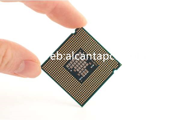
Le substrat du boîtier Ajinomoto GX92R est un composant clé largement utilisé dans l'industrie électronique moderne. C'est un panneau plat fait d'un matériau non conducteur, utilisant souvent de la fibre de verre, matériaux époxy ou composites pour sa structure de base. Ces matériaux sont soigneusement sélectionnés pour garantir que le substrat présente une résistance mécanique et une stabilité suffisantes tout en ayant de bonnes propriétés d'isolation électrique..
La surface du substrat du boîtier Ajinomoto GX92R est plaquée ou imprimée avec des chemins conducteurs, qu'on appelle des traces. Des traces se forment à la surface du substrat grâce à des processus de gravure chimique ou d'impression, et ils sont responsables de la connexion des composants électroniques et des circuits du bâtiment pour mettre en œuvre les fonctions de l'appareil. La conception et la disposition de ces traces sont cruciales et affectent directement les performances et la stabilité du circuit.. Donc, les concepteurs doivent prendre en compte des facteurs tels que la connexion électrique entre les composants, la vitesse et la stabilité de la transmission du signal, etc.. lors de la conception du substrat du boîtier Ajinomoto GX92R pour assurer le fonctionnement normal de l'ensemble du circuit.
Les connexions électriques du substrat du boîtier Ajinomoto GX92R assurent non seulement la connectivité entre les composants, mais également entreprendre les tâches importantes de transmission de signaux et d'alimentation électrique. Cela signifie que les traces doivent avoir une conductivité électrique suffisante et être capables de maintenir des performances électriques stables dans différents environnements de travail.. En outre, la conception du substrat du boîtier Ajinomoto GX92R doit également prendre en compte des facteurs tels que la gestion thermique pour garantir de bonnes performances en fonctionnement à haute température ou à haute puissance.
En général, le substrat d'emballage Ajinomoto GX92R fait partie intégrante de l'équipement électronique et joue un rôle important dans la connexion et le support de divers composants électroniques. Sa conception et sa fabrication nécessitent une technologie hautement professionnelle et une fabrication précise pour garantir que le produit final présente d'excellentes performances et stabilité..
Guide de référence de conception du substrat du package Ajinomoto GX92R.
La conception du package Ajinomoto GX92R substrat est un élément crucial du développement des équipements électroniques. Il s'agit de la disposition des composants électroniques et du routage des connexions électriques sur la carte., qui ont tous deux un impact direct sur la fonctionnalité et les performances du produit final. Pendant le processus de conception, plusieurs facteurs doivent être pris en compte pour assurer la stabilité, fiabilité et performances supérieures du substrat d’emballage.
D'abord, le placement des composants est l'une des considérations importantes dans le processus de conception. Un placement correct des composants peut minimiser l'utilisation de l'espace sur le circuit imprimé et garantir une bonne gestion thermique et l'intégrité du signal entre les composants.. En examinant attentivement l'emplacement et la disposition des composants, vous pouvez optimiser les performances de la carte et augmenter la fiabilité globale du système.
Deuxièmement, l'intégrité du signal est l'une des questions sur lesquelles il faut se concentrer pendant le processus de conception. Une bonne intégrité du signal garantit que les signaux ne sont pas perturbés ou perdus pendant la transmission sur le circuit imprimé., assurant ainsi la stabilité et la fiabilité du système. Pendant le processus de conception, des mesures doivent être prises pour réduire la diaphonie du signal, retard du signal, et distorsion du signal pour garantir des performances élevées et une fiabilité élevée du circuit imprimé.
En outre, la gestion thermique est également l'un des facteurs à prendre en compte lors du processus de conception. Pendant le fonctionnement des équipements électroniques, les composants du circuit imprimé généreront de la chaleur. Si la gestion thermique ne peut pas être réalisée efficacement, cela peut provoquer une surchauffe des composants, affectant ainsi les performances et la stabilité du système. Donc, il est nécessaire de disposer rationnellement le radiateur et le ventilateur pendant le processus de conception, et prendre d'autres mesures efficaces de dissipation thermique pour assurer le fonctionnement normal du circuit imprimé.
Enfin, la fabricabilité est l'un des facteurs à prendre en compte lors du processus de conception. Le circuit imprimé conçu doit être facile à fabriquer et à assembler pour garantir un processus de production fluide et minimiser les coûts de production.. Pendant le processus de conception, les limites du processus de fabrication doivent être prises en compte et les matériaux et processus appropriés doivent être sélectionnés pour garantir la qualité et la fiabilité du circuit imprimé..
En résumé, la conception du substrat du boîtier Ajinomoto GX92R nécessite une prise en compte approfondie de plusieurs facteurs, y compris le placement des composants, intégrité du signal, gestion thermique, et fabricabilité. Ce n'est qu'en prenant pleinement en compte ces facteurs que nous pourrons concevoir un système stable., substrat d'emballage fiable et aux performances supérieures pour fournir un support fiable pour le développement d'équipements électroniques.
Quel matériau est utilisé dans le substrat du package Ajinomoto GX92R?
Les substrats du boîtier Ajinomoto GX92R utilisent souvent une variété de matériaux dans leur fabrication, dont la plus courante est la résine époxy renforcée de fibre de verre (FR4). FR4 est un matériau composite haute performance doté d'excellentes propriétés mécaniques et électriques, adapté à la plupart des applications électroniques..
Les principales caractéristiques du matériau FR4 incluent une haute résistance, résistance à la chaleur, résistance chimique et bonne isolation électrique, ce qui en fait l'un des matériaux préférés pour la fabrication de PCB. Sa fiabilité et sa stabilité font que le FR4 est souvent utilisé dans des applications nécessitant une haute qualité et une stabilité à long terme.
En plus de FR4, Les substrats du boîtier Ajinomoto GX92R sont également disponibles dans d'autres matériaux en fonction des besoins spécifiques de l'application.. L'un d'eux est un matériau céramique, qui a une bonne résistance aux températures élevées et à la corrosion et est largement utilisé dans les équipements électroniques haute fréquence et haute puissance.
Une autre option est le polyimide (PI) matériel, qui a une excellente résistance aux températures élevées, résistance chimique et résistance mécanique et convient aux environnements de travail difficiles tels que les industries aérospatiale et automobile.
En outre, les matériaux à base de métal sont également un choix courant, spécialement pour les appareils électroniques de haute puissance qui nécessitent de bonnes performances de dissipation thermique. Les PCB à base de métal ont d'excellentes propriétés de conductivité thermique et peuvent transférer efficacement la chaleur des composants électroniques vers le dissipateur thermique ou le boîtier pour garantir la stabilité et la longue durée de vie de l'appareil..
Dans l'ensemble, le substrat du boîtier Ajinomoto GX92R permet une sélection de matériaux flexible en fonction des besoins spécifiques de l'application pour garantir des performances optimales, fiabilité et durabilité. Que vous choisissiez FR4, céramique, substrats en polyimide ou en métal, ils peuvent être personnalisés pour répondre aux exigences d'une variété d'appareils et de systèmes électroniques.
Quelle est la taille du substrat du package Ajinomoto GX92R?
Les tailles de substrat du boîtier Ajinomoto GX92R varient en fonction de l'application spécifique et de la taille de l'appareil ou du système électronique.. Cette polyvalence le rend idéal pour une variété de scénarios. Poussé par la technologie moderne, la taille et les exigences fonctionnelles des appareils électroniques sont de plus en plus diversifiées, la taille des substrats d'emballage doit donc également s'adapter à ce changement en conséquence.
Pour les petits appareils électroniques, tels que les téléphones mobiles et les appareils portables, Les substrats du boîtier Ajinomoto GX92R doivent souvent être petits, fin et léger pour répondre aux exigences de conception compacte de l'appareil. De tels substrats d'emballage doivent accueillir divers composants électroniques dans un espace limité et doivent maintenir des performances et une fiabilité suffisantes..
Au contraire, pour de grands scénarios d'application tels que les équipements industriels et les infrastructures de télécommunications, le substrat d'emballage Ajinomoto GX92R peut nécessiter une taille plus grande et une capacité de charge plus élevée pour accueillir davantage de composants électroniques et de conceptions de circuits complexes. Ces grands substrats d'emballage sont généralement conçus pour résister à des conditions environnementales industrielles difficiles telles que des températures élevées., haute pression, et aux chocs mécaniques tout en maintenant des performances et une fiabilité stables.
Quelle que soit la taille, Les substrats du boîtier Ajinomoto GX92R doivent répondre à des normes de performance et à des exigences de qualité strictes.. Pendant le processus de conception, les ingénieurs doivent prendre en compte de manière exhaustive divers facteurs, y compris la disposition du circuit, conception thermique, intégrité du signal et résistance mécanique, etc., pour garantir que le substrat d'emballage peut fonctionner de manière stable et fiable dans divers environnements d'application.
En résumé, Les substrats du boîtier Ajinomoto GX92R sont disponibles dans une large gamme de tailles, vous permettant de trouver une solution adaptée, des petits appareils portables aux grands systèmes industriels. Cette flexibilité fait du substrat d'emballage Ajinomoto GX92R un composant clé indispensable dans les équipements et systèmes électroniques modernes., fournissant des connexions électriques stables et fiables et une transmission du signal pour divers scénarios d'application.
Le processus de fabrication du substrat du package Ajinomoto GX92R.
Le processus de fabrication du substrat du boîtier Ajinomoto GX92R est un processus précis et complexe impliquant plusieurs étapes critiques pour garantir la qualité et les performances du produit final.. Les étapes clés seront présentées en détail ci-dessous:
Préparation du substrat: La première étape du processus de fabrication consiste à préparer le substrat, utilisant généralement des matériaux tels que l'époxy renforcé de fibre de verre (FR4). Le substrat doit être nettoyé et la surface préparée pour garantir que les étapes ultérieures de revêtement et de gravure puissent se dérouler sans problème..
Alignement des calques: Pendant l’étape d’alignement des calques, les couches individuelles d'un substrat multicouche doivent être alignées avec précision pour garantir que les chemins conducteurs suivants peuvent connecter correctement les composants électroniques entre les différentes couches.
Gravure ou impression de chemins conducteurs: Vient ensuite la création de chemins conducteurs, qui est l’une des étapes les plus critiques du processus de fabrication. Selon les exigences de conception, des chemins conducteurs sont formés sur la surface du substrat par gravure ou impression, et ces chemins seront utilisés pour connecter divers composants électroniques.
Perçage des trous des composants: Une fois les chemins conducteurs formés, des trous doivent être percés dans le substrat pour monter les composants électroniques. Ces trous doivent être positionnés avec précision et garantir qu'ils correspondent aux chemins conducteurs pour l'installation et la connexion ultérieures des composants..
Application du film tampon: L'application du film de tampon vise à fournir une bonne surface de soudure après l'installation des composants. Cette étape consiste généralement à placer un film de tampon autour des chemins conducteurs et des trous des composants pour garantir une connexion soudée fiable et stable..
Assemblage de composants: Une fois le substrat préparé, les composants électroniques sont montés avec précision dans leurs positions désignées. Ce processus nécessite un équipement et une technologie automatisés très sophistiqués pour garantir une installation et un positionnement corrects des composants..
Essai: Après fabrication, le substrat d'emballage est soumis à des tests rigoureux pour vérifier ses performances et sa fiabilité. Les tests incluent les tests fonctionnels, tests électriques, tests de fiabilité, etc.. pour garantir que le substrat d'emballage répond aux exigences de conception et aux normes de l'industrie.
Dans l'ensemble, le processus de fabrication du substrat du boîtier Ajinomoto GX92R nécessite un haut niveau de technologie et de savoir-faire, couvrant plusieurs étapes clés. Grâce à des processus de fabrication précis, de haute qualité, des substrats d'emballage hautement fiables peuvent être produits, fournir un support fiable pour le fonctionnement stable de divers appareils et systèmes électroniques.
Le domaine d'application du substrat du package Ajinomoto GX92R.
Les substrats d'emballage Ajinomoto GX92R jouent un rôle important dans diverses industries et sont utilisés dans un large éventail de domaines, notamment l'électronique grand public., automobile, aérospatial, équipement médical, télécommunications et automatisation industrielle.
Dans le domaine de l'électronique grand public, Les substrats d'emballage Ajinomoto GX92R sont largement utilisés dans divers smartphones, comprimés, appareils portables et appareils électroménagers. En tant que composants essentiels des équipements électroniques, ils assurent des performances stables et un fonctionnement efficace de l'équipement.
Dans l'industrie automobile, Les substrats du boîtier Ajinomoto GX92R sont utilisés dans les systèmes de contrôle électronique automobile, systèmes de divertissement embarqués, et électronique du corps. Ils effectuent le traitement des données des capteurs, fonctions de communication et de contrôle, améliorer la sécurité, confort et intelligence de la voiture.
Dans le champ aérospatial, Les substrats d'emballage Ajinomoto GX92R sont utilisés dans les systèmes de commandes de vol, systèmes de navigation et systèmes de communication. Ils sont légers, très fiable et résistant aux radiations, ce qui les rend adaptés aux exigences environnementales strictes de l'aérospatiale.
Dans le domaine des dispositifs médicaux, Les substrats du boîtier Ajinomoto GX92R sont utilisés dans les équipements d'imagerie médicale, systèmes de surveillance des patients, et équipement de diagnostic médical. Ils ont des exigences extrêmement élevées en matière de traitement des données de haute précision et de stabilité., assurer l’exactitude et la fiabilité des équipements médicaux.
Dans le domaine des télécommunications, Les substrats du boîtier Ajinomoto GX92R sont utilisés dans les stations de base de communication, équipement de communication par fibre optique et routeurs de réseau. Ils prennent en charge la transmission de données à haut débit et les protocoles de communication complexes, assurer le fonctionnement stable des réseaux de communication.
Dans le domaine de l'automatisation industrielle, Les substrats d'emballage Ajinomoto GX92R sont utilisés dans les robots industriels, Systèmes de contrôle PLC et réseaux de capteurs. Ils assurent les tâches de contrôle et de surveillance des équipements industriels, améliorer l'efficacité de la production et la qualité de la fabrication.
Dans l'ensemble, l'utilisation généralisée des substrats du boîtier Ajinomoto GX92R permet aux appareils et systèmes électroniques de diverses industries d'atteindre des performances plus élevées, fonctionnement plus fiable, et une gamme d'applications plus large.
Quels sont les avantages du substrat du package Ajinomoto GX92R?
Les avantages du substrat du boîtier Ajinomoto GX92R sont évidents et il joue un rôle essentiel dans la conception et la fabrication d'appareils électroniques modernes.. Le substrat du boîtier Ajinomoto GX92R offre de multiples avantages par rapport aux autres méthodes de routage, voici quelques-uns des principaux:
D'abord, le substrat du boîtier Ajinomoto GX92R est petit. Alors que les appareils électroniques deviennent de plus en plus minces, plus léger, et plus portable, l'utilisation de l'espace pour les composants internes est devenue de plus en plus importante. Ce substrat d'emballage peut remplir plus de fonctions dans un espace limité et aider à concevoir des produits plus compacts et plus élégants..
Deuxièmement, le substrat du boîtier Ajinomoto GX92R offre une grande fiabilité. Grâce à des processus de fabrication précis et à un contrôle qualité, ce substrat d'emballage assure la stabilité et la fiabilité à long terme des appareils électroniques. Ils sont capables de résister aux défis de diverses conditions environnementales, comme les changements de température, humidité et contraintes mécaniques, prolongeant ainsi la durée de vie de l'équipement.
En outre, le substrat du boîtier Ajinomoto GX92R est facile à produire en série. Utiliser des processus de production modernes et des équipements automatisés, ce substrat d'emballage peut être produit à grande échelle, réduisant ainsi les coûts de production et améliorant l'efficacité de la production. Cette capacité de production de masse permet aux fabricants d'équipements électroniques de répondre à la demande du marché en temps opportun et de conserver un avantage concurrentiel..
Le substrat du boîtier Ajinomoto GX92R réduit également les erreurs d'assemblage. En montant des composants électroniques directement sur le substrat, les erreurs et les fautes lors de l'assemblage manuel peuvent être réduites. Cela contribue à améliorer l’efficacité de la production, réduire les coûts de fabrication des produits, et assurer la performance et la fiabilité des équipements.
En plus, le substrat du boîtier Ajinomoto GX92R améliore l'intégrité du signal. Grâce à une conception et un câblage soignés, les interférences et la distorsion du signal peuvent être minimisées, assurer la stabilité et la fiabilité de l'appareil lors de la transmission de données et de l'exécution de fonctions. Ceci est particulièrement important pour les appareils électroniques hautes performances et haute fréquence..
Enfin, le substrat du boîtier Ajinomoto GX92R présente des performances thermiques améliorées. Une bonne conception de conduction thermique et de dissipation thermique peut transférer efficacement la chaleur des composants électroniques vers l'environnement environnant, empêcher l'équipement de surchauffer et améliorer son efficacité et sa fiabilité de fonctionnement. Ceci est particulièrement critique pour les équipements qui nécessitent de longues périodes de fonctionnement ou une puissance de sortie élevée..
Dans l'ensemble, les avantages du substrat du boîtier Ajinomoto GX92R ne se reflètent pas seulement dans sa petite taille et sa grande fiabilité, mais aussi en termes de facilité de production en série, Erreurs d'assemblage réduites, Amélioration de l'intégrité du signal, et des performances thermiques améliorées. Cela en fait l’un des composants privilégiés dans la conception et la fabrication d’équipements électroniques modernes., stimuler le progrès continu et l’innovation technologique.
FAQ
En quoi la base de package Ajinomoto GX92R est-elle différente des autres bases de package?
Le substrat d'emballage Ajinomoto GX92R utilise des matériaux de haute qualité et des processus de fabrication avancés pour offrir de meilleures performances électriques et thermiques.. Sa conception spéciale et sa sélection de matériaux lui permettent de bien fonctionner à haute fréquence, températures élevées et environnements complexes, il est donc plus populaire dans certaines applications qui nécessitent une plus grande stabilité.
Comment choisir l'épaisseur appropriée du substrat d'emballage?
Le choix de l'épaisseur du substrat du boîtier dépend des besoins de l'application et des exigences de conception.. En général, des substrats plus minces peuvent offrir une meilleure conductivité thermique et une densité plus élevée, mais peut sacrifier une certaine résistance mécanique. Donc, lors de la sélection de l'épaisseur du substrat d'emballage, un équilibre entre l'électricité, les propriétés thermiques et mécaniques doivent être prises en compte.
Quelle est la température de fonctionnement maximale du substrat du boîtier Ajinomoto GX92R?
La température de fonctionnement maximale du substrat du boîtier Ajinomoto GX92R dépend de son matériau et de sa conception., et il peut généralement fonctionner de manière stable dans la plage de températures de -40°C à +150°C. Cependant, pour certaines applications spéciales, des conceptions personnalisées peuvent être nécessaires pour répondre à des exigences de température plus élevées.
Comment garantir la fiabilité des substrats d'emballage?
Pour assurer la fiabilité des substrats d’emballage, un contrôle de qualité strict est requis pendant les processus de conception et de fabrication. Cela inclut l'utilisation de matériaux de haute qualité, procédés de fabrication de précision, tests de qualité stricts et respect des normes et spécifications pertinentes. En outre, tests de fiabilité appropriés, tels que les tests de cycle de température, essai de vibration, et tests d'humidité, doit être effectué pour vérifier la stabilité du substrat de l'emballage dans diverses conditions environnementales.
Le substrat du boîtier Ajinomoto GX92R est-il recyclable?
Oui, Les substrats du boîtier Ajinomoto GX92R sont généralement fabriqués à partir de matériaux respectueux de l'environnement et peuvent être recyclés via des processus de manipulation et de recyclage appropriés.. Cela contribue à réduire l’impact environnemental et à parvenir à une utilisation durable des ressources..