CO., LTD")
Fabrication de PCB à cavités, Les PCB à cavité ouverte nécessitent une découpe contrôlée en profondeur pour exposer les couches internes à l'air pour l'assemblage de l'antenne ou des composants..
Circuit imprimé multicouche avec cavités. nous avons réalisé de nombreuses cavités sur le circuit imprimé vierge. Haute qualité, Livraison rapide, et un prix encore moins cher. Notre Entreprise de PCB a produit Circuit de cavité depuis 4 couche à 50 couches. À propos des matériaux des circuits de cavité. si vous n'avez besoin que du PCB avec des matériaux de base FR4. nous les terminerons rapidement. par exemple: 4 couche à 8 panneaux de cavité de couche. nous les terminerons dans 10 à 15 jours. depuis 10 couche à 20 couches planches à cavité. nous avons besoin d'environ 15 à 20 jours.
les cartes à cavité avec des matériaux PCB spéciaux. par exemple: Matériaux de circuits haute performance, Matériaux des circuits FR4 à faible perte, Matériaux pour circuits à grande vitesse, Matériaux des circuits haute fréquence. le délai sera un peu long. peut-être besoin d'environ 15 à 30 jours. avant de nous envoyer les fichiers gerber. si vous avez des questions. veuillez vérifier auprès de notre équipe d'ingénieurs. À propos des matériaux PCB. nous avons de nombreux matériaux de circuits spéciaux dans notre entrepôt. certains sont très chers. certains sont moins chers. si vous utilisez un noyau FR4 standard pour réaliser les cartes des cavités. le prix sera encore moins cher. si vous utilisez Noyau haute vitesse ou haute fréquence. le prix du PCB sera cher. les matériaux ne sont pas les mêmes. donc. le prix ne sera pas le même.
LeTechnologies PCB pour cavités. Oui. nous pouvons fabriquer les panneaux creux avec de nombreuses technologies avancées. Exemple: Nous pouvons fabriquer le circuit imprimé de cavité avec des vias enterrés et aveugles. s'il te plaît, fais attention pour savoir. dans la zone des cavités. il y a des trous de vias enterrés ou aveugles. je veux dire. les vias montreront le côté extérieur du cuivre dans la zone de la cavité.
À propos des matériaux diélectriques. si tu as besoin. nous pouvons fabriquer le circuit imprimé des cavités avec de nombreux matériaux diélectriques différents. comme: Diélectriques Rogers Diélectriques VS FR4, Ou, Diélectriques Rogers VS diélectriques Isola, Ou M7, M4, Diélectriques M6, et d'autresHautes performances, Diélectriques FR4 à faibles pertes. Dites-nous simplement. de quels types de diélectriques avez-vous besoin ?? dis-nous s'il te plaît. nous pouvons le produire. et fais du bon travail.
À propos des autres technologies de production de PCB à cavité. comme: Contrôle de l'impédance. nous pouvons faire +/-5%, Cachot, Exercice et déroute de profondeur contrôlée, Rigide & Circuits flexibles, et d'autres. notre société a fabriqué de nombreux produits militaires PCB, PCB aéronautique, PCB de communication militaire, Produit PCB industriel, et de nombreux produits dans d'autres domaines.
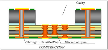
Qu'est-ce qu'un PCB à cavité?
Un PCB à cavité, également connu sous le nom de panneau à cavité ou panneau à dos creux, est un type de carte de circuit imprimé avec une zone ou une cavité en retrait usinée sur un ou deux côtés. Cette zone encastrée peut varier en profondeur et en forme en fonction des exigences spécifiques de l'application..
Construction de PCB à cavité: Les PCB à cavité sont généralement construits à l'aide de techniques traditionnelles de fabrication de PCB., avec l'étape supplémentaire de fraisage ou de fraisage d'une cavité sur un ou les deux côtés de la planche. Cette cavité peut être usinée à des dimensions précises à l'aide de CNC (Commande numérique par ordinateur) machines ou autres équipements de fabrication avancés. Le substrat PCB restant forme la base ou les parois de la cavité, assurer l’intégrité structurelle du conseil d’administration.
Applications des PCB à cavité: Les PCB à cavité trouvent des applications dans diverses industries où des conceptions spécialisées sont nécessaires pour répondre à des critères de performance spécifiques.. Certaines applications courantes incluent:
- Systèmes d'antennes: Les PCB à cavité sont largement utilisés en RF (Radiofréquence) et applications micro-ondes, en particulier dans les systèmes d'antennes. La cavité fait office de bouclier, réduire les interférences électromagnétiques (EMI) et améliorer les performances de l'antenne.
- Circuits haute fréquence: En raison de leurs propriétés supérieures d’intégrité du signal, les PCB à cavité sont utilisés dans les circuits haute fréquence tels que les systèmes radar, équipement de télécommunications, et appareils sans fil.
- Aéronautique et Défense: Les industries de l'aérospatiale et de la défense utilisent des PCB à cavité dans des systèmes critiques où la fiabilité, durabilité, et la performance sont primordiales. Ces cartes sont souvent déployées en avionique, systèmes radar, et systèmes de guidage de missiles.
- Dispositifs médicaux: En électronique médicale, en particulier dans les équipements de diagnostic et les appareils d'imagerie, les PCB à cavité offrent une clarté de signal améliorée et une réduction du bruit, contribuant à des lectures et des diagnostics plus précis.
Avantages des PCB à cavité: L'utilisation de PCB à cavité offre plusieurs avantages, y compris:
- Intégrité du signal améliorée: La conception de la cavité réduit les interférences électromagnétiques, assurant une transmission et une réception de signal plus propres, surtout dans les applications à haute fréquence.
- Gestion thermique améliorée: Les PCB à cavité facilitent une dissipation thermique plus efficace, crucial pour les composants électroniques fonctionnant dans des environnements exigeants.
- Optimisation de l'espace: En intégrant des composants dans la cavité, les circuits imprimés à cavité permettent des conceptions compactes et légères, idéal pour les applications à espace limité telles que les appareils électroniques portables et les systèmes aérospatiaux.
Considérations pour la conception de circuits imprimés à cavité: Alors que les PCB à cavité offrent de nombreux avantages, certaines considérations doivent être prises en compte lors du processus de conception et de fabrication:
- Coût: L'usinage des cavités augmente le coût de fabrication des PCB, ce qui rend les cartes à cavités plus chères que les PCB standards.
- Stabilité mécanique: Une attention particulière doit être accordée à l'intégrité mécanique des PCB à cavité pour garantir qu'ils peuvent résister aux contraintes environnementales et maintenir la stabilité structurelle..
Conclusion: Les PCB à cavité représentent une solution spécialisée adaptée aux applications exigeantes nécessitant des performances élevées, fiabilité, et l'intégrité du signal. Avec leur conception et leur construction uniques, ces conseils jouent un rôle essentiel dans diverses industries, y compris les télécommunications, aérospatial, défense, et électronique médicale, stimuler l’innovation et le progrès dans les systèmes électroniques.
Comment concevoir un PCB: Un guide étape par étape?
Introduction: Concevoir un circuit imprimé (PCB) est une étape cruciale dans le développement des appareils électroniques. Que vous soyez un ingénieur chevronné ou un passionné novice, comprendre les principes fondamentaux de la conception de PCB est essentiel. Ce guide vous guidera à travers le processus de conception d'un PCB, de la conceptualisation à la fabrication, mettre en évidence les étapes et les considérations clés tout au long du processus.
Étape 1: Définir les exigences avant de plonger dans le processus de conception, définir clairement les exigences de votre PCB. Tenez compte de facteurs tels que les contraintes de taille, spécifications électriques, placement des composants, et conditions environnementales dans lesquelles le PCB fonctionnera.
Étape 2: Conception schématique Créez un diagramme schématique de votre circuit à l'aide d'EDA (Automatisation de la conception électronique) des logiciels tels qu'Altium Designer, Aigle, ou KiCad. Ce schéma sert de modèle pour les connexions entre les composants et définit le comportement électrique du circuit..
Étape 3: Sélection et placement des composants Choisissez les composants requis pour votre circuit en fonction de leur fonctionnalité, disponibilité, et le coût. Une fois sélectionné, placer les composants sur la disposition du PCB selon le diagramme schématique. Tenez compte de facteurs tels que le routage du signal, gestion thermique, et facilité d'assemblage lors du placement des composants.
Étape 4: Disposition du PCB Avec les composants placés, passer à l'étape de configuration du PCB. Disposez les composants sur le PCB pour optimiser l'intégrité du signal, minimiser les interférences, et assurer un routage efficace. Faites attention à des facteurs tels que la longueur de la trace, contrôle d'impédance, et chemins de retour du signal lors de la conception du réseau.
Étape 5: Routage Connectez les composants sur le schéma PCB en acheminant les traces entre eux. Suivez les meilleures pratiques pour le routage des traces, comme le maintien de largeurs de trace cohérentes, éviter les angles vifs, et minimiser la diaphonie du signal. Utilisez des plans de masse et d'alimentation pour fournir une distribution de tension stable et réduire les interférences électromagnétiques.
Étape 6: Vérification des règles de conception (RDC) Effectuez une vérification des règles de conception pour vous assurer que la conception de votre PCB est conforme aux contraintes de fabrication et aux normes de l'industrie.. Cela inclut la vérification des violations d'autorisation, largeurs de trace minimales, et tailles de tampons correctes. Traiter toute erreur ou avertissement identifié au cours du processus DRC.
Étape 7: Vérification de la conception avant de procéder à la fabrication, vérifier la fonctionnalité et l'intégrité de votre conception de PCB grâce à la simulation et aux tests. Utiliser ÉPICES (Programme de simulation axé sur les circuits intégrés) logiciel pour simuler le comportement du circuit et valider les performances par rapport aux spécifications de conception. Prototyper et tester le PCB pour identifier tout problème et apporter les ajustements nécessaires.
Étape 8: Générez des fichiers de fabrication Une fois la conception de votre PCB finalisée et vérifiée, générer les fichiers de fabrication nécessaires à la fabrication. Ces fichiers incluent généralement des fichiers Gerber pour les illustrations de PCB, limes de perçage pour le placement des trous, et une nomenclature (Nomenclature) détailler les spécifications des composants. Examinez les fichiers de fabrication pour garantir leur exactitude avant de les envoyer au fabricant de PCB.
Étape 9: Fabrication et assemblage Soumettre les fichiers de fabrication à une usine de fabrication de PCB pour la production. Choisissez un fabricant réputé qui offre des services de fabrication de qualité et respecte vos spécifications. Dès réception des PCB fabriqués, procéder à l'assemblage et au soudage des composants conformément à la nomenclature et aux instructions d'assemblage.
Conclusion: La conception d'un PCB nécessite une planification minutieuse, attention aux détails, et le respect des bonnes pratiques. En suivant ce guide étape par étape, vous pouvez créer un PCB bien conçu qui répond aux exigences de votre projet et fonctionne de manière fiable dans son application prévue. Affinez continuellement vos compétences en conception et restez informé des avancées de la technologie PCB pour relever en toute confiance des défis de conception de plus en plus complexes..
Comment fabriquer PCB de la cavité?
Un guide complet sur la fabrication de PCB à cavité: Introduction: PCB de cavité, connu pour sa conception spécialisée comportant des zones encastrées, offrir des performances améliorées dans diverses applications électroniques. La fabrication de ces cartes nécessite précision et expertise pour obtenir une fonctionnalité optimale. Ce guide fournit un aperçu détaillé du processus de fabrication des PCB à cavité, couvrant les étapes et considérations clés.
Étape 1: Conception et ingénierie Le processus de fabrication des PCB à cavité commence par une conception et une ingénierie complètes. Les ingénieurs planifient soigneusement la disposition, en tenant compte de facteurs tels que les dimensions de la cavité, sélection des matériaux, et exigences électriques. CAO spécialisée (Conception Assistée par Ordinateur) le logiciel est utilisé pour créer des conceptions précises qui répondent aux spécifications de l'application prévue.
Étape 2: Sélection des matériaux La sélection des matériaux appropriés est essentielle pour la fabrication de circuits imprimés à cavité. Matériaux de substrat de haute qualité, comme FR-4 (Ignifuge 4), PTFE (Polytétrafluoroéthylène), ou en céramique, sont couramment utilisés pour leur stabilité thermique, propriétés diélectriques, et résistance mécanique. En plus, les matériaux conducteurs pour les traces de circuit et les plots de composants sont choisis en fonction de la conductivité, résistance à la corrosion, et compatibilité avec le processus de fabrication.
Étape 3: Usinage de cavités La caractéristique déterminante des PCB à cavité est la zone en retrait usinée dans la carte.. Cette étape implique un usinage de précision à l'aide de CNC (Commande numérique par ordinateur) équipements ou fraiseuses spécialisées. Les dimensions de la cavité doivent s'aligner précisément sur les spécifications de conception pour garantir un ajustement et une fonctionnalité appropriés des composants.. Une attention particulière est portée au maintien de l'uniformité et de la douceur des parois de la cavité afin d'éviter les faiblesses structurelles ou les interférences de signal..
Étape 4: Alignement et liaison des couches dans les PCB à cavités multicouches, les couches individuelles sont alignées et liées ensemble pour former une structure unifiée. L'alignement est crucial pour garantir un enregistrement correct des traces conductrices et des vias à travers les couches. Diverses techniques de collage, comme le laminage ou le collage, sont utilisés en fonction des matériaux du substrat et des exigences de conception. Une liaison appropriée garantit l'intégrité structurelle et la continuité électrique dans tout le PCB.
Étape 5: Création de circuits et gravure Une fois les couches de substrat liées, les modèles de circuit sont transférés sur la surface du PCB. Cela se fait généralement à l'aide d'un masque photorésistant et d'un processus de gravure.. La résine photosensible est appliquée sur le substrat, exposé à la lumière UV à travers un photomasque, et développé pour révéler le modèle de circuit souhaité. Les zones exposées sont ensuite gravées à l'aide de solutions chimiques, laissant derrière lui les traces conductrices et les plots de composants.
Étape 6: Placage et finition de surface Surfaces conductrices du PCB, y compris les traces de circuit et les plots de composants, sont plaqués de métal pour améliorer la conductivité et la durabilité. Les métaux de placage courants comprennent le cuivre, nickel, et de l'or. Techniques de finition de surface, comme HASL (Nivellement de la soudure à air chaud), Accepter (Or d'immersion nickel électrolaire), ou OSP (Conservateur de soudabilité organique), sont appliqués pour protéger les surfaces exposées de l’oxydation et faciliter la brasage pendant l’assemblage.
Étape 7: Assurance qualité et tests tout au long du processus de fabrication, des mesures d'assurance qualité sont mises en œuvre pour garantir l'intégrité et la fonctionnalité des PCB de la cavité. Inspection visuelle, mesures dimensionnelles, tests électriques, et des analyses thermiques sont effectuées à différentes étapes pour détecter et rectifier tout défaut ou écart par rapport aux spécifications. Des tests complets valident les performances et la fiabilité des PCB finis avant qu'ils ne soient libérés pour assemblage et intégration dans des systèmes électroniques..
Conclusion: La fabrication de PCB à cavité nécessite une combinaison de technologies avancées, ingénierie de précision, et des mesures strictes de contrôle de la qualité. En suivant le processus décrit et en tirant parti de l'expertise en science des matériaux et en techniques de fabrication, les fabricants peuvent produire des circuits imprimés à cavité de haute qualité qui répondent aux exigences exigeantes des applications électroniques modernes. L'innovation et le perfectionnement continus des pratiques de fabrication améliorent encore les performances et la polyvalence des PCB à cavité dans diverses industries.
Nous pouvons produire de nombreux types de cavités dans les cartes PCB à haute couche. Si vous avez des questions, N'hésitez pas à nous contacter avecinfo@alcantapcb.com , Nous serons heureux de vous aider.