CO., LTD")
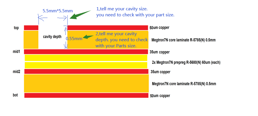
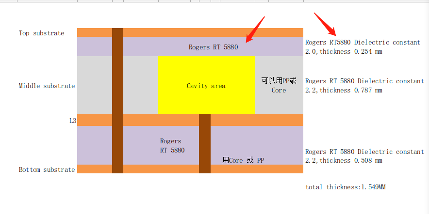
PCB de la cavité introduction. un type est une cavité ouverte sur les PCB. ou peut-être ouvrir plusieurs cavités sur les planches. et l'autre est la cavité enterrée. ça veut dire. L'emplacement vide se situe entre la couche moyenne et la couche moyenne. nous pouvons produire ces deux types de PCB à cavité à partir de 4 couche à 50 couches.
Dans le domaine de l'électronique moderne, cartes de circuits imprimés (PCBS) jouer un rôle essentiel en garantissant la fonctionnalité et l’efficacité des appareils électroniques. Parmi les diverses technologies de fabrication de PCB, La technologie Cavity PCB se distingue par ses avantages uniques en termes de performances, fiabilité et miniaturisation et est considéré comme une approche innovante. Dans ce guide complet, nous plongeons dans les subtilités de la fabrication de la technologie des PCB à cavité, explorer ses composants clés, processus de fabrication, matériels, facteurs de coût, et les entreprises qui pilotent sa croissance.
Qu'est-ce que la technologie des PCB à cavité?
Technologie des PCB à cavité, PCB à composants intégrés ou carte à cavité, est une technologie avancée de fabrication électronique conçue pour surmonter les limitations d'espace et les contraintes de poids auxquelles sont confrontés les montages en surface traditionnels. (Smt) technologie. Par rapport aux méthodes traditionnelles d'assemblage de surfaces, La technologie des PCB à cavité atteint la compacité, légèreté et hautes performances des appareils électroniques en intégrant des composants dans les couches du substrat PCB. Cette technologie est principalement utilisée dans des scénarios nécessitant des exigences strictes en matière d'espace et de poids., comme l'aérospatiale, équipement médical, électronique automobile et électronique grand public portable.
Technologie PCB dans la cavité, les composants sont intégrés dans les couches internes du PCB plutôt que d'être apposés sur la surface du PCB via la technologie de montage en surface. Cette conception permet de réduire la taille globale de l'appareil électronique, économisant ainsi de l'espace et réduisant également le poids de l'appareil. En même temps, parce que les composants sont intégrés à l'intérieur du PCB, leur zone de contact avec le milieu extérieur est réduite, réduisant ainsi l'impact des dommages mécaniques et des facteurs environnementaux sur les composants, et améliorer la fiabilité et la durabilité des équipements.
La technologie des PCB à cavité a une large gamme d'applications. Dans le champ aérospatial, cette technologie est utilisée pour fabriquer des équipements avioniques légers et performants, tels que les systèmes de commandes de vol, équipement de communication, et systèmes de navigation. Dans le domaine du matériel médical, La technologie Cavity PCB est utilisée pour fabriquer des équipements de surveillance médicale et des instruments de diagnostic compacts et fiables., comme les stimulateurs cardiaques, équipement d'imagerie médicale et capteurs médicaux implantables. Dans le domaine de l'électronique automobile, La technologie Cavity PCB est utilisée pour fabriquer des systèmes électroniques automobiles légers et hautes performances., tels que les unités de commande du véhicule, systèmes d'aide à la conduite et systèmes de divertissement pour véhicules. En outre, appareils électroniques grand public portables, comme les smartphones, tablettes et appareils portables, sont également des scénarios d'application typiques de la technologie Cavity PCB. Son design compact et ses caractéristiques hautes performances répondent aux besoins des consommateurs modernes en matière de portabilité et de fonctionnalité..
En général, l'émergence de la technologie Cavity PCB a apporté de nouvelles possibilités dans le domaine de la fabrication électronique. En intégrant des composants dans des PCB, l'équipement électronique a été rendu compact, léger et performant, fournir de l'innovation technologique dans diverses industries. et mises à niveau de produits.
Comment concevoir un PCB à cavité?
La conception d'un PCB à cavité est une tâche qui nécessite une planification et une réflexion minutieuses car elle implique de nombreux facteurs clés qui ont un impact direct sur les performances et la fiabilité de la carte.. Les principales considérations pour la conception d'un PCB à cavité sont explorées en détail ci-dessous:
Tout d'abord, Le placement des composants est la clé de la conception de PCB à cavité. Lors de la disposition des composants, vous devez considérer la relation spatiale entre eux et leur distance par rapport à la cavité. Une disposition raisonnable des composants peut minimiser la taille du circuit imprimé et garantir le chemin de connexion le plus court entre les composants, réduisant ainsi le délai et la perte de transmission du signal.
Deuxièmement, la gestion thermique est l'une des questions sur lesquelles il faut se concentrer lors de la conception de PCB à cavité. Étant donné que les PCB à cavité intègrent généralement un grand nombre de composants et de circuits, une grande quantité de chaleur est générée pendant le fonctionnement. Mesures efficaces de gestion thermique, comme les dissipateurs de chaleur, dissipateurs de chaleur, caloducs, etc., peut aider à conduire et à dissiper efficacement la chaleur et à empêcher les circuits imprimés d'être endommagés en raison d'une surchauffe.
L'intégrité du signal est un autre facteur qui nécessite une attention particulière. Lors de la conception de PCB à cavité, vous devez vous assurer que la disposition et le routage des lignes de signal répondent aux exigences d'intégrité du signal afin d'éviter les interférences ou la distorsion du signal. À l'aide d'outils de simulation avancés, le chemin de transmission du signal peut être analysé et optimisé pour garantir que la carte de circuit imprimé maintient une qualité de signal stable dans des conditions de transmission à haute fréquence et à grande vitesse.
La fabricabilité est l'une des dernières considérations lors de la conception de PCB à cavité. Il est nécessaire de s'assurer que la conception répond aux exigences du processus de fabrication pour éviter des difficultés de fabrication ou des conceptions irréalisables.. Pendant le processus de conception, les limites du processus de fabrication et de l'équipement doivent être prises en considération, et des matériaux et processus appropriés doivent être sélectionnés pour garantir que le circuit imprimé peut être produit et assemblé en douceur.
En général, la conception de PCB à cavité nécessite une prise en compte approfondie de plusieurs aspects tels que le placement des composants, gestion thermique, intégrité du signal, et fabricabilité. Avec un logiciel avancé de conception de PCB et des outils de simulation, les concepteurs peuvent optimiser la disposition et le routage pour garantir des performances et une fiabilité optimales de la carte.
Quel est le processus de fabrication des PCB à cavité?
Le processus de fabrication des PCB à cavité est un projet précis et complexe qui nécessite plusieurs étapes critiques pour obtenir un produit de haute qualité. Ce qui suit est une analyse détaillée du processus de fabrication des PCB à cavité:
La première étape de la fabrication du PCB à cavité consiste à préparer le substrat. Des matériaux de substrat de haute qualité sont généralement utilisés, comme la résine renforcée de fibre de verre (FR-4) ou stratifiés haute fréquence. Le substrat doit être nettoyé et préparé en surface pour garantir une bonne adhérence et une bonne planéité de la surface..
Une fois la préparation du substrat terminée, différentes couches de matériaux sont laminées selon les exigences de conception. Ces couches peuvent inclure une feuille de cuivre, couches d'isolation, et couches diélectriques spéciales. L'ordre et l'épaisseur de l'empilement affectent les performances et la fonctionnalité du PCB final..
Une fois le lay-up terminé, la prochaine étape critique est le fraisage de la cavité. C'est l'élément central de la technologie Cavity PCB, dans lequel des machines sophistiquées découpent des cavités ou des rainures profondes dans la couche interne du PCB selon les exigences de conception pour accueillir les composants intégrés.
Une fois le fraisage de la cavité terminé, les composants sont précisément intégrés dans les couches internes du PCB. Ces composants peuvent être des puces, inductances, condensateurs ou autres composants microscopiques. L'emplacement et la disposition des composants intégrés doivent être strictement conformes aux exigences de conception pour garantir une bonne connexion électrique et de bonnes performances..
Une fois les composants intégrés, les différentes couches du PCB seront laminées ensemble. Pendant le processus de laminage, le PCB est soumis à des températures et des pressions élevées afin que les matériaux entre les couches puissent être fermement liés pour former une structure globale solide et fiable.
Enfin, le PCB passera par les dernières étapes de finition, y compris les bords de coupe, percer des trous, appliquer des couches de protection, etc.. Ces étapes permettent de garantir que l'apparence et les dimensions du PCB répondent aux exigences de conception et augmentent sa durabilité et sa fiabilité..
Tout au long du processus de fabrication, il est crucial d'utiliser des équipements et des technologies de fabrication professionnels pour garantir la précision et la cohérence du processus de production.. En même temps, des mesures de contrôle de qualité strictes et une surveillance des processus sont également des facteurs clés pour garantir la qualité des PCB à cavité. Grâce à un travail soigné et une gestion stricte de la qualité, les fabricants sont en mesure de produire des produits PCB à cavité qui répondent à des normes élevées et répondent aux besoins et aux attentes des clients.
Comment est fabriqué le PCB à cavité?
La fabrication de PCB à cavité implique l'intégration de technologies et de processus de fabrication avancés pour obtenir une qualité et des performances supérieures.. De la conception initiale au produit final, chaque étape du processus est critique. D'abord, l'équipe de conception doit planifier soigneusement la disposition du PCB de la cavité, prise en compte des emplacements d'intégration des composants, Chemins de transmission du signal, gestion thermique, et faisabilité de fabrication. Utilisation d'un logiciel avancé de conception de PCB et d'outils de simulation, ils peuvent simuler les performances de différentes solutions pendant la phase de conception pour garantir que la meilleure solution de conception est sélectionnée.
Une fois la conception terminée, le processus de fabrication commence. Dans les usines modernes, les lignes d'assemblage automatisées jouent un rôle clé. D'abord, selon le dossier de conception, le substrat du PCB à cavité est transformé en la forme et la taille requises grâce à un usinage précis. Suivant, selon les exigences de conception, les cavités sont fraisées dans des couches spécifiques du substrat pour intégrer les composants. Cette étape nécessite un équipement d'usinage de haute précision et un contrôle strict pour garantir que la taille et l'emplacement de la cavité sont conformes à la conception..
Une fois la cavité prête, l'intégration des composants peut commencer. Cela peut impliquer de coller le composant sur un substrat, puis de l'intégrer dans la cavité en utilisant la pression ou la chaleur.. Un contrôle et une surveillance précis sont cruciaux au cours de ce processus pour garantir que les composants sont correctement intégrés et bien connectés aux matériaux environnants..
Ensuite, un processus de laminage a lieu, presser les différentes couches de substrat et les composants intégrés ensemble. Cela nécessite un contrôle précis de la température et de la pression pour garantir des connexions solides entre les couches sans endommager les composants intégrés.. Une fois le laminage terminé, le PCB de la cavité est coupé à sa forme et à sa taille finales par découpe et finition, et reçu un traitement de surface final pour améliorer son apparence et sa durabilité.
Des mesures strictes de contrôle de qualité font partie intégrante de tout le processus de fabrication.. Grâce à l'utilisation d'équipements et de technologies de test avancés, chaque étape de fabrication est surveillée et inspectée pour garantir que les produits répondent aux normes de qualité les plus élevées. Ce n'est que lorsque la qualité est garantie que Cavity PCB peut répondre aux besoins des clients et exercer ses avantages dans divers scénarios d'application..
Quelles sont les considérations de coût pour les PCB à cavité?
Le coût de fabrication des PCB à cavité est l’un des facteurs clés affectant sa compétitivité sur le marché. Bien que les PCB à cavité offrent des avantages inégalés en termes de performances et de miniaturisation, ils peuvent nécessiter des coûts de fabrication plus élevés que les PCB traditionnels. Lorsque l'on considère le coût du PCB à cavité, les facteurs suivants nécessitent une attention particulière:
La sélection des matériaux de PCB de cavité est essentielle à son coût. Les matériaux de haute qualité ont généralement de meilleures propriétés électriques, stabilité thermique, et résistance mécanique, mais ils ont aussi tendance à être plus chers. Le type et la qualité des matériaux utilisés dans le processus de fabrication affectent directement les performances et la fiabilité des PCB à cavité, l'équilibre entre coût et qualité doit donc être soigneusement pesé lors de la sélection des matériaux.
La complexité de la conception des PCB à cavité est un autre facteur important affectant les coûts. Les conceptions de PCB à cavité sont généralement plus complexes et nécessitent plus de temps et de ressources en raison des composants intégrés et des connexions intercouches complexes.. Les conceptions complexes peuvent nécessiter des techniques d'ingénierie plus avancées et davantage d'étapes de fabrication., augmentation des coûts de fabrication.
Le volume de production est l'un des facteurs importants affectant le coût des PCB à cavité. Typiquement, la production en grand volume réduit les coûts de fabrication par unité car les coûts fixes peuvent être répartis sur un plus grand nombre de produits. Cependant, pour une production en faible volume ou des projets personnalisés, le coût unitaire peut être plus élevé car les coûts fixes doivent être répartis sur un plus petit nombre de produits.
La fabrication de PCB à cavité peut nécessiter une technologie et des équipements avancés pour mettre en œuvre des composants intégrés et des connexions intercouches complexes. Les investissements dans ces technologies et équipements peuvent augmenter les coûts de fabrication, surtout lors de la première utilisation. En outre, les ressources humaines nécessaires à la formation et aux compétences spécialisées augmentent également les coûts de fabrication.
Donc, pour tout projet de PCB à cavité, le coût de fabrication est un facteur clé qui doit être soigneusement pris en compte et évalué. Au moment de décider d'adopter la technologie Cavity PCB, les fabricants doivent prendre en compte de manière exhaustive les facteurs ci-dessus et garantir une rentabilité optimale tout en garantissant la qualité et les performances des produits..
Quels matériaux sont utilisés dans les PCB à cavité?
Les PCB à cavité sont généralement fabriqués à partir de matériaux de haute qualité, dont FR-4, Rogers, et stratifiés haute fréquence, entre autres. Ces matériaux jouent un rôle clé dans la fabrication de PCB à cavité, fournir une base solide pour la performance et la fiabilité des appareils électroniques.
D'abord, FR-4 est un substrat courant en résine époxy renforcée de fibre de verre avec d'excellentes propriétés électriques et résistance mécanique.. Il est largement utilisé dans la fabrication de circuits imprimés à cavité en raison de sa capacité à fournir de bonnes propriétés d'isolation et à prévenir efficacement les interférences de signal et les fuites électriques.. La stabilité et la durabilité des matériaux FR-4 en font le premier choix dans l'aérospatiale, automobile, et matériel médical.
Deuxièmement, Le matériau Rogers est un type spécial de matériau de carte de circuit imprimé haute fréquence avec d'excellentes propriétés diélectriques et caractéristiques de transmission du signal.. Les matériaux Rogers sont largement utilisés dans les communications haute fréquence et les systèmes radar en raison de leurs faibles pertes., faible constante diélectrique et performances stables. Fabrication de PCB dans la cavité, Les matériaux Rogers peuvent être utilisés pour obtenir une transmission de signal à plus haute fréquence et réduire la perte de signal, améliorant ainsi les performances et la stabilité du circuit.
En outre, le stratifié haute fréquence est un matériau spécial conçu pour les circuits haute fréquence, généralement fabriqué à partir de plastiques hautes performances tels que le PTFE (polytétrafluoroéthylène) ou PP (polypropylène). Ces matériaux ont d'excellentes propriétés diélectriques, stabilité thermique et chimique, et conviennent à une utilisation dans diverses conditions environnementales difficiles. Fabrication de PCB dans la cavité, les stratifiés haute fréquence peuvent être utilisés pour obtenir des fréquences plus élevées et des conceptions de circuits plus complexes afin de répondre aux besoins en dispositifs électroniques hautes performances dans des domaines tels que les communications, aérospatial, et matériel médical.
Dans l'ensemble, Les PCB à cavité sont généralement fabriqués à partir de matériaux de haute qualité tels que le FR-4, Rogers, et stratifiés haute fréquence, qui ont d'excellentes propriétés électriques, stabilité thermique, et résistance mécanique, ce qui les rend idéaux pour une variété de scénarios d'application exigeants. En sélectionnant des matériaux appropriés et en les combinant avec des procédés de fabrication avancés, Les fabricants de PCB à cavité sont en mesure de fournir à leurs clients des performances élevées, solutions d'appareils électroniques fiables et stables.
Qui sont les principaux fabricants de PCB à cavité?
La fabrication de PCB à cavité englobe une gamme de processus et de technologies sophistiqués conçus pour permettre une intégration transparente de composants intégrés afin d'améliorer les performances et la fiabilité des appareils électroniques.. En tant que fournisseur de fabrication de PCB à cavité, notre société possède une vaste expérience et expertise et s'engage à fournir à ses clients des produits de haute qualité, des solutions innovantes.
D'abord, la première étape de la fabrication des PCB à cavité consiste à préparer le substrat. Nous choisissons des matériaux de substrat de haute qualité, comme FR-4 ou Rogers, pour garantir que le PCB fabriqué présente de bonnes caractéristiques électriques et une bonne résistance mécanique. Nous utilisons ensuite une technologie de stratification avancée pour empiler les différentes couches afin de fournir une base solide pour les composants intégrés à monter..
Le fraisage des cavités est une étape cruciale dans le processus de fabrication des PCB à cavité. Nous utilisons un équipement de fraisage de précision pour créer des cavités dans la couche interne du PCB selon les exigences de conception afin d'accueillir les composants intégrés.. Cela garantit une liaison étroite entre le composant et le PCB tout en minimisant la taille et le poids global du PCB..
Vient ensuite l’installation des composants embarqués. Nous installons et connectons avec précision les composants à leurs emplacements désignés via des lignes d'assemblage automatisées avancées. Des procédures strictes de contrôle de qualité garantissent que chaque composant est installé conformément aux spécifications de conception et garantissent la fiabilité et la stabilité du produit final..
Au stade final de la fabrication des PCB à cavité, nous effectuons des processus de laminage et de finition. Par l'action de la haute température et de la haute pression, il assure la liaison étroite entre les différentes couches, tout en offrant une finition lisse à la surface du PCB pour un assemblage et une utilisation ultérieurs.
En tant que fournisseur de fabrication de PCB à cavité, nous nous engageons à améliorer continuellement la qualité des produits et la satisfaction des clients grâce à une innovation continue et une mise à niveau technologique. Notre équipe de professionnels vous fournira de tout cœur des solutions personnalisées et travaillera en étroite collaboration avec vous pour promouvoir conjointement le développement et le progrès de l'industrie électronique..
Quelles sont les qualités d'un bon service client?
Fabrication de PCB dans la cavité, un excellent service client est un facteur clé pour garantir la satisfaction et la fidélité des clients. Une communication efficace est la pierre angulaire d’une bonne relation client. Les fabricants doivent être capables de comprendre clairement les besoins et les exigences des clients et de fournir des informations et des solutions précises en temps opportun.. Communiquer ne signifie pas seulement écouter les opinions et les commentaires des clients, mais aussi être capable de communiquer de manière proactive avec les clients et de partager l'avancement du projet et les risques possibles pour garantir que les clients comprennent toujours l'état du projet.
La réactivité est un autre aspect crucial. Lorsque les clients soulèvent des questions ou des besoins, ils s'attendent à recevoir des réponses et des solutions en temps opportun. Les fabricants doivent établir un mécanisme de retour d'information efficace pour garantir que les problèmes des clients peuvent être traités et résolus en temps opportun.. Des réponses rapides et précises renforcent la confiance des clients dans les fabricants et augmentent la satisfaction des clients.
L'expertise technique fait partie intégrante du service client. Les fabricants doivent posséder des connaissances et une expérience techniques approfondies et être en mesure de fournir aux clients des conseils et une assistance professionnels.. Qu'il s'agisse de consultation technique lors de la phase de conception ou d'assistance technique pendant le processus de fabrication, les fabricants doivent être capables de comprendre avec précision les besoins des clients et de fournir les solutions correspondantes.
La fiabilité est l'un des attributs clés du service client. Les fabricants doivent faire preuve d'une attitude de travail fiable et d'un engagement pour garantir la confiance des clients dans leurs produits et services.. Cela inclut la livraison des produits à temps, garantir la qualité des produits et respecter les obligations contractuelles. Grâce à des performances fiables, les fabricants peuvent gagner la confiance de leurs clients et construire des solutions à long terme, des relations solides.
L'engagement envers la qualité est un autre aspect important du service client. Les fabricants doivent toujours viser l’excellence en matière de qualité et améliorer continuellement la qualité des produits et les processus de fabrication.. Les clients n'attendent pas seulement des produits, mais aussi des solutions fiables et stables. Par la recherche incessante de la qualité, les fabricants peuvent gagner la confiance et le respect des clients et établir une bonne image de marque.
En résumé, un excellent service client dans la fabrication de PCB à cavité exige que les fabricants possèdent des attributs clés tels qu'une communication efficace, réactivité, expertise technique, fiabilité et engagement envers la qualité. Ces qualités aident non seulement les fabricants à établir de bonnes relations avec leurs clients, mais également favoriser une collaboration à long terme et un succès mutuel.
Questions fréquemment posées
Quels sont les principaux avantages de l'utilisation de la technologie Cavity PCB?
La technologie Cavity PCB offre plusieurs avantages clés, y compris une miniaturisation améliorée, gestion thermique améliorée, réduction des interférences électromagnétiques (EMI), et une fiabilité accrue. En intégrant des composants dans le substrat PCB, Les PCB à cavité permettent la création de dispositifs électroniques compacts et légers avec des performances optimisées.
En quoi la technologie des PCB à cavité diffère-t-elle de la fabrication conventionnelle de PCB?
Contrairement aux méthodes conventionnelles de fabrication de PCB qui impliquent le montage de composants sur la surface de la carte, La technologie Cavity PCB intègre des composants dans les couches du substrat. Cette approche élimine le besoin de composants externes volumineux, réduit les interférences du signal, et améliore la fiabilité et la durabilité globales de l'appareil électronique.
Quelles industries utilisent couramment des PCB à cavité dans leurs produits?
Les PCB à cavité trouvent des applications dans diverses industries, y compris l'aérospatiale, automobile, dispositifs médicaux, télécommunications, et l'électronique grand public. Ces industries nécessitent souvent des solutions électroniques compactes et légères, offrant des performances et une fiabilité élevées., faisant des PCB à cavité un choix idéal pour leurs produits.
Quels facteurs influencent le coût de fabrication des PCB à cavité?
Le coût de fabrication des PCB à cavité dépend de plusieurs facteurs, y compris la complexité de la conception, le type et la qualité des matériaux utilisés, le volume de production, et la technologie et l'équipement requis. En général, Les PCB à cavité peuvent entraîner des coûts de fabrication plus élevés que les PCB conventionnels en raison des étapes supplémentaires impliquées dans l'intégration des composants dans le substrat..
Comment puis-je sélectionner le bon fabricant pour mon projet de PCB à cavité?
Lors du choix d'un fabricant pour votre projet de PCB à cavité, prendre en compte des facteurs tels que l'expérience et l'expertise du fabricant dans la technologie des PCB à cavité, leurs capacités et installations de fabrication, leurs processus de contrôle qualité, leur expérience en matière de fourniture de produits de haute qualité, et leur capacité à répondre à vos exigences et délais spécifiques. Il est essentiel d’effectuer des recherches approfondies et de demander des devis et des échantillons à plusieurs fabricants pour prendre une décision éclairée..