CO., LTD")
Fabricante de PCB de cavidade. PCBs de cavidade aberta exigem um recorte com profundidade controlada para expor as camadas internas ao ar para montagem de antena ou componente. A fábrica de PCB de Alcanta produz muitos tipos de placas PCB de cavidade. Cavidades em placas PCB. A maior parte do design. você tem que colocar algum IC principal (peças) nas cavidades. Sim. podemos produzir esse tipo Placas de cavidade com alta qualidade. podemos fazer a cavidade pcb de 4 camada para 70 camadas. a maior parte da cavidade é de 4 camada para 16 camadas.
Em algum domínio especial. A placa de cavidades usará materiais de placa de circuito impresso de alta velocidade, Materiais PCB de alta frequência, Materiais de metal, Materiais de alto TG FR4, ou outros materiais PCB diferentes. podemos produzir todos esses tipos de placas de cavidades de materiais. Alta qualidade, e preço mais barato. Quando você projeta este tipo de PCB de cavidades. se você tiver alguma dúvida. você pode verificar conosco. nós vamos ajudá-lo a qualquer momento. não há necessidade de qualquer pagamento. Apenas troca técnica.

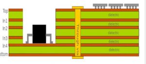
O Tecnologias de PCB para cavidades. Sim. podemos fazer placas de cavidades com muitas tecnologias avançadas. Exemplo: Podemos fazer a placa de cavidade com vias enterradas e cegas. por favor preste atenção para saber. na área das cavidades. existem alguns buracos de Vias Enterrados ou Cegos. quero dizer. os orifícios de passagem mostrarão o lado do cobre na área da cavidade.
Sobre os materiais dielétricos. se você precisar. podemos fazer a placa de cavidades com muitos materiais dielétricos diferentes. como: Dielétricos de Rogers Dielétricos VS FR4, Ou, Dielétricos Rogers VS Dielétricos Isola, Ou M7, M4, Dielétricos M6, e outro Alto desempenho, Dielétricos FR4 de baixa perda. Apenas diga-nos. que tipos de dielétricos você precisa, por favor? diga-nos por favor. podemos produzi-lo. e faça um bom trabalho.
Sobre outras tecnologias de produção de PCB de cavidade. como: Controle de Impedância. podemos fazer +/-5%, Perfuração posterior, Perfuração e roteamento de profundidade controlada, Rígido-Flex & Circuitos Flexíveis, e outros. nossa empresa produziu muitos produtos PCB militares, PCB de aviação, PCB de comunicação militar, Produto PCB industrial, e muitos produtos em outros campos.
Outras mais informações sobre PCBs de cavidade: O que é PCB de cavidade?
No mundo dinâmico da eletrônica, a inovação é constante, dando origem a tecnologias especializadas como PCBs de cavidade. Essas placas de circuito exclusivas oferecem vantagens distintas em aplicações específicas, revolucionando indústrias onde a precisão e o desempenho são fundamentais. Este artigo investiga o conceito de PCBs de cavidade, lançando luz sobre sua construção, aplicações, e benefícios.
Compreendendo PCBs de cavidade: PCBs de cavidade, também conhecidos como PCBs com suporte de cavidade ou placas de cavidade, são um tipo especializado de placa de circuito impresso com uma ou mais áreas rebaixadas, ou cavidades, usinado em um ou ambos os lados. Essas regiões rebaixadas podem variar em forma, profundidade, e tamanho, dependendo dos requisitos da aplicação.
Construção de PCBs de cavidade: A construção de PCBs com cavidade envolve processos tradicionais de fabricação de PCB com uma etapa adicional – fresamento ou roteamento de cavidades na superfície da placa(s). CNC avançado (Controle Numérico Computadorizado) equipamentos de usinagem ou fresagem esculpem com precisão essas cavidades, deixando para trás o substrato que forma a base ou paredes da cavidade. Este processo meticuloso garante a integridade estrutural ao mesmo tempo que acomoda os requisitos de design especializados do PCB.
Aplicações de PCBs de cavidade: Os PCBs de cavidade são amplamente utilizados em vários setores onde o desempenho, confiabilidade, e a integridade do sinal são críticas. Algumas aplicações proeminentes incluem:
- Sistemas de RF e Microondas: PCBs de cavidade são excelentes em aplicações de RF e micro-ondas, particularmente em sistemas de antenas e equipamentos de comunicação. A cavidade funciona como um escudo, minimizando a interferência eletromagnética e melhorando a transmissão e recepção do sinal.
- Eletrônica de alta frequência: Em circuitos de alta frequência, como sistemas de radar, dispositivos sem fio, e comunicações satélites, PCBs de cavidade oferecem desempenho superior, reduzindo a perda de sinal e o ruído, melhorando assim a eficiência geral do sistema.
- Aeroespacial e Defesa: Os setores aeroespacial e de defesa utilizam PCBs de cavidade em sistemas de missão crítica, como aviônicos, matrizes de radar, e sistemas de orientação de mísseis. Seu design robusto e excepcional integridade de sinal os tornam indispensáveis nesses ambientes exigentes.
- Eletrônica Médica: Em dispositivos médicos e equipamentos de diagnóstico, PCBs de cavidade desempenham um papel vital na garantia de leituras e diagnósticos precisos. Sua capacidade de minimizar interferências e manter a clareza do sinal é inestimável em aplicações médicas sensíveis.
Benefícios dos PCBs de cavidade: PCBs de cavidade oferecem vários benefícios importantes, incluindo:
- Integridade de sinal aprimorada: O design da cavidade reduz a interferência eletromagnética, resultando em uma transmissão de sinal mais limpa e melhor desempenho geral, particularmente em aplicações de alta frequência.
- Gerenciamento térmico aprimorado: PCBs de cavidade facilitam melhor dissipação de calor, crucial para componentes eletrônicos que operam em ambientes térmicos desafiadores, aumentando assim a confiabilidade e a longevidade do sistema.
- Otimização de Espaço: Integrando componentes dentro da cavidade, PCBs de cavidade permitem designs compactos e leves, tornando-os ideais para aplicações com espaço limitado onde tamanho e peso são fatores críticos.
Conclusão: Os PCBs de cavidade representam uma solução especializada adaptada às demandas exclusivas dos sistemas eletrônicos modernos. Com seu design avançado, construção precisa, e características de desempenho superiores, PCBs de cavidade continuam a impulsionar a inovação em uma ampla gama de indústrias, ampliando os limites do que é possível em design e fabricação eletrônica.
Como projetar um PCB?
Projetando um PCB: Um guia abrangente:
Projetando uma placa de circuito impresso (PCB) é uma habilidade fundamental para entusiastas e profissionais de eletrônica. Esteja você criando um projeto de hobby simples ou um dispositivo eletrônico complexo, compreender o processo de design de PCB é essencial. Este artigo fornece um guia conciso, porém abrangente, para projetar um PCB, cobrindo as principais etapas e considerações ao longo do caminho.
Etapa 1: Defina os requisitos Comece definindo claramente os requisitos do seu PCB. Considere fatores como o tamanho, funcionalidade, Requisitos de energia, e condições ambientais em que irá operar. Compreender esses requisitos antecipadamente guiará todo o processo de design.
Etapa 2: Projeto esquemático Crie um diagrama esquemático do seu circuito usando Electronic Design Automation (EDA) programas. Este esquema serve como um modelo para as conexões entre os componentes e define o comportamento elétrico do circuito. Garanta precisão e integridade na fase de projeto esquemático.
Etapa 3: Seleção e posicionamento de componentes Selecione componentes com base em sua funcionalidade, disponibilidade, e custo. Uma vez escolhido, coloque os componentes no layout da PCB de acordo com o diagrama esquemático. Considere fatores como roteamento de sinal, gerenciamento térmico, e facilidade de montagem durante a colocação de componentes.
Etapa 4: Layout da PCB Prossiga para a etapa de layout da PCB após colocar os componentes. Organize os componentes na PCB para otimizar a integridade do sinal, minimizar a interferência, e garantir roteamento eficiente. Preste atenção a fatores como comprimento do traço, controle de impedância, e caminhos de retorno de sinal durante o design do layout.
Etapa 5: Roteamento Conecte os componentes no layout da PCB roteando traços entre eles. Siga as práticas recomendadas para roteamento de rastreamento, como manter larguras de traço consistentes, evitando cantos afiados, e minimizando a diafonia do sinal. Use planos de aterramento e energia para fornecer distribuição de tensão estável e reduzir a interferência eletromagnética.
Etapa 6: Verificação de regras de design (RDC) Execute uma verificação de regras de projeto para garantir que seu projeto de PCB esteja em conformidade com as restrições de fabricação e os padrões da indústria. Verifique se há violações de autorização, larguras mínimas de traço, e tamanhos corretos de almofadas. Resolva quaisquer erros ou avisos identificados durante o processo de RDC.
Etapa 7: Verificação do projeto antes da fabricação, verifique a funcionalidade e integridade do seu projeto de PCB por meio de simulação e testes. Use software de simulação para validar o desempenho em relação às especificações do projeto. Prototipar e testar o PCB para identificar quaisquer problemas e fazer os ajustes necessários.
Etapa 8: Gere arquivos de fabricação depois de finalizado e verificado, gerar os arquivos de fabricação necessários para fabricação. Esses arquivos normalmente incluem arquivos Gerber para arte de PCB, limas de perfuração para colocação de furos, e uma lista de materiais (BOM) detalhando especificações de componentes. Revise a precisão dos arquivos de fabricação antes de enviá-los ao fabricante da PCB.
Etapa 9: Fabricação e montagem Envie os arquivos de fabricação para uma instalação de fabricação de PCB para produção. Escolha um fabricante confiável que ofereça serviços de fabricação de qualidade. Ao receber os PCBs fabricados, prossiga com a montagem e soldagem dos componentes de acordo com a lista técnica e as instruções de montagem.
Conclusão: Projetar um PCB requer um planejamento cuidadoso, atenção aos detalhes, e adesão às melhores práticas. Seguindo este guia, você pode criar uma PCB bem projetada que atenda aos requisitos do seu projeto e tenha um desempenho confiável na aplicação pretendida. Aprimore continuamente suas habilidades de design e mantenha-se atualizado com os avanços na tecnologia de PCB para enfrentar desafios de design cada vez mais complexos com confiança.
Como fabricar uma PCB de cavidade?
Processo de fabricação de PCBs de cavidade: Um guia abrangente:
PCBs de cavidade, também conhecidos como PCBs com suporte de cavidade, representam um tipo especializado de placa de circuito impresso com áreas rebaixadas ou cavidades usinadas em um ou ambos os lados. O processo de fabricação de PCBs de cavidade envolve etapas exclusivas para obter precisão e confiabilidade. Este artigo fornece uma visão geral do processo de fabricação, destacando as principais etapas e considerações.
Etapa 1: Projeto e Especificação O processo de fabricação de PCBs de cavidade começa com a fase de projeto, onde os engenheiros definem o layout, dimensões, e especificações da placa. Isto inclui determinar a localização, tamanho, e profundidade das cavidades, bem como selecionar materiais e acabamentos que atendam aos requisitos da aplicação.
Etapa 2: Seleção de materiais A seleção do material de substrato apropriado é crucial para PCBs de cavidade. Materiais comuns incluem FR-4, Rogers, e alta frequência laminados, escolhido com base em fatores como constante dielétrica, condutividade térmica, e força mecânica. O material do substrato fornece a base para o PCB e influencia suas propriedades elétricas e mecânicas.
Etapa 3: Usinagem CNC Assim que o projeto e a seleção do material forem finalizados, o processo de fabricação passa para CNC (Controle Numérico Computadorizado) usinagem. Usando equipamentos de fresagem ou roteamento de precisão, os técnicos esculpem cuidadosamente as cavidades no substrato do PCB de acordo com as especificações do projeto. A usinagem CNC garante precisão e consistência nas dimensões e posicionamento da cavidade.
Etapa 4: Empilhamento e laminação de camadas após usinagem das cavidades, a próxima etapa é empilhamento e laminação de camadas. Múltiplas camadas de folha de cobre e pré-impregnado são imprensadas entre as camadas de substrato para formar o empilhamento de PCB. Este empilhamento é então prensado sob alta temperatura e pressão usando um processo de laminação, unindo as camadas em uma única, estrutura coesa.
Etapa 5: Perfuração e chapeamento Depois que o empilhamento de PCB for laminado, equipamento de perfuração de precisão é usado para criar furos para montagem de componentes e conexões elétricas. Depois de perfurar, os furos são revestidos com cobre para estabelecer a condutividade elétrica e garantir interconexões confiáveis entre as camadas.
Etapa 6: Padronização e gravação de circuitos O próximo estágio envolve padronizar os traços e recursos do circuito nas camadas do PCB.. Um material fotorresistente é aplicado às superfícies de cobre, seguido de exposição à luz UV através de uma fotomáscara, que define o padrão de circuito desejado. As áreas expostas são então gravadas com soluções químicas, deixando para trás os traços e características de cobre desejados.
Etapa 7: Acabamento de superfície e montagem após gravação, o PCB passa por processos de acabamento superficial para proteger os vestígios de cobre e melhorar a soldabilidade. Acabamentos de superfície comuns incluem HASL (Nivelamento de solda de ar quente), Concordar (Ouro de imersão em níquel eletrolítico), e OSP (Conservantes orgânicos de soldabilidade). Finalmente, os componentes são montados no PCB usando máquinas automatizadas de coleta e colocação, e soldado no lugar usando técnicas de soldagem por refluxo ou soldagem por onda.
Conclusão: O processo de fabricação de PCBs de cavidade exige precisão, experiência, e atenção aos detalhes em cada etapa. Do design e seleção de materiais à usinagem CNC, laminação, e montagem, cada estágio desempenha um papel crucial na produção de PCBs de cavidade de alta qualidade que atendem aos rigorosos requisitos das aplicações eletrônicas modernas. Seguindo as melhores práticas e aproveitando tecnologias avançadas de fabricação, os fabricantes podem garantir a confiabilidade e o desempenho de PCBs de cavidade em vários setores.
Podemos produzir vários tipos de cavidades em placas PCB de alta camada. Se você tiver quaisquer perguntas, não hesite em contactar-nos com info@alcantapcb.com , teremos prazer em ajudá-lo.