CO., LTD")
Substratos e embalagens cerâmicas. Fabricação de substratos para embalagens de materiais de alta velocidade e alta frequência. Processo e tecnologia avançada de produção de substrato de embalagem.
Cerâmica, frequentemente associado à fragilidade e habilidade artística, realmente ocupam um lugar central no domínio da eletrônica. Além de seus aspectos decorativos, cerâmicas servem como componentes essenciais em uma ampla gama de aplicações eletrônicas. Este artigo oferece uma exploração esclarecedora no domínio dos substratos e embalagens cerâmicas, amplamente empregado em vários domínios eletrônicos. Em nosso mundo contemporâneo, dispositivos eletrônicos se integraram perfeitamente à vida diária, abrangendo smartphones, sistemas de controle automotivo, equipamento de comunicação, e instrumentos médicos. Em meio a esta vasta e intricada paisagem, cerâmica surge como material indispensável, com suas propriedades e atributos distintivos, posicionando-os como a melhor escolha para fabricação de eletrônicos.
A cerâmica é reverenciada por sua excepcional estabilidade em temperaturas elevadas, propriedades isolantes, robustez mecânica, e inércia química. Esses atributos tornam a cerâmica uma escolha ideal para componentes eletrônicos, particularmente em ambientes exigentes caracterizados por altas temperaturas, frequências, e pressões. As capacidades de isolamento da cerâmica são fundamentais na prevenção de interferências entre componentes eletrônicos, melhorando assim a estabilidade do circuito e o desempenho geral.
Adicionalmente, exploraremos como as embalagens cerâmicas são fundamentais em dispositivos eletrônicos projetados para operar sob condições extremas de temperatura e frequência. À medida que a tecnologia continua sua evolução implacável, o escopo de aplicações para cerâmica continua a se expandir. Este artigo serve como sua porta de entrada para este domínio fascinante, oferecendo insights sobre como a cerâmica impulsiona a inovação e o progresso na indústria eletrônica.
À medida que você avança neste artigo, você cultivará uma compreensão mais profunda da cerâmica’ importância central na eletrônica e desenvolver uma apreciação pelos papéis críticos da inovação e das práticas sustentáveis no avanço do setor eletrônico. Junte-se a nós nesta exploração do mundo da cerâmica e descubra as suas possibilidades ilimitadas.
Aplicação de substratos cerâmicos na área eletrônica
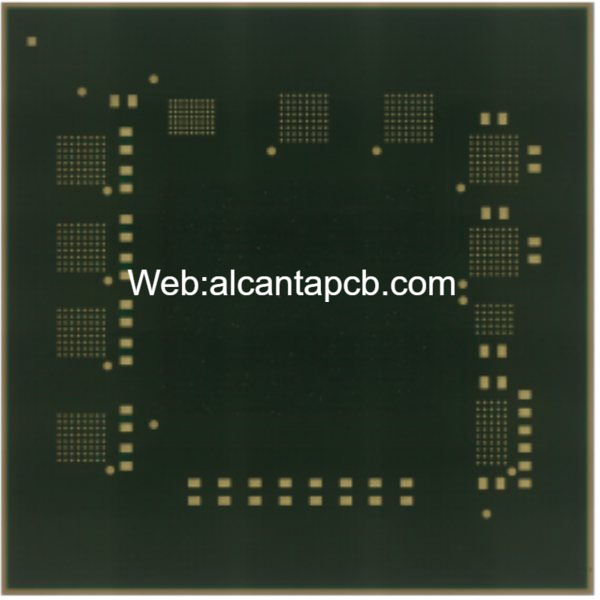
Os substratos cerâmicos representam uma tecnologia fundamental no domínio da eletrônica. Suas estruturas e propriedades distintas os tornam um elemento indispensável em uma infinidade de dispositivos eletrônicos. Neste segmento, embarcaremos em uma extensa exploração dos princípios fundamentais que sustentam os substratos cerâmicos, sua contribuição vital para o cenário da fabricação de eletrônicos, e nos aprofundaremos em aplicações do mundo real, abrangendo casos como placas de circuito impresso (PCB) e sensores.
Conceitos básicos e estruturas de substratos cerâmicos
Os substratos cerâmicos são normalmente fabricados a partir de materiais cerâmicos isolantes, como óxido de alumínio. (Al2O3) ou nitreto de silício (Si3N4). Sua construção normalmente envolve múltiplas camadas de cerâmica intrinsecamente unidas por meio de adesivos e processos de fabricação especializados.. Esta arquitetura multicamadas assume um papel significativo em aplicações eletrônicas, pois não apenas fornece isolamento elétrico, mas também se destaca em condutividade térmica, ao mesmo tempo que exibe notável robustez mecânica.
O papel fundamental dos substratos cerâmicos na fabricação de eletrônicos
Substratos cerâmicos são essenciais para o cenário da fabricação de eletrônicos. Eles encontram ampla utilização no suporte e interconexão de diversos componentes eletrônicos, incluindo circuitos integrados, resistores, capacitores, e vários outros elementos. Esses substratos fornecem uma plataforma robusta para a montagem e conectividade desses componentes, garantindo sua funcionalidade ideal.
Além disso, substratos cerâmicos se destacam na condução e dissipação de calor. Eles transferem calor com eficiência para o ambiente circundante, contribuindo assim para a manutenção do desempenho estável em dispositivos eletrônicos. Esta capacidade é particularmente significativa em aplicações eletrônicas de alta potência, como módulos de potência e amplificadores.
Placas de Circuito Impresso (PCB): No reino da fabricação de PCB, substratos cerâmicos assumem um papel fundamental. Eles servem como substrato fundamental para PCBs, fornecendo isolamento elétrico e condutividade térmica. Esta configuração é particularmente adequada para componentes eletrônicos de alta frequência, conforme evidenciado em equipamentos de comunicação e radiofrequência (RF) aplicações.
Sensores: Substratos cerâmicos desfrutam de ampla aplicação em tecnologia de sensores. Por exemplo, ambientes de alta temperatura e alta pressão utilizam substratos cerâmicos em sensores de pressão Shell para medir mudanças de pressão. As propriedades isolantes e termicamente condutoras dos substratos cerâmicos os tornam ideais para uma ampla gama de sensores, sensores de temperatura abrangentes, acelerômetros, e sensores de gás.
Em essência, substratos cerâmicos desempenham um papel insubstituível no domínio da fabricação eletrônica. Sua estrutura e propriedades distintas os tornam adequados para uma variedade de aplicações, abrangendo desde PCBs até sensores e desde eletrônicos de alta frequência até os desafios impostos por condições de alta temperatura e alta pressão. Esses substratos servem como motores vitais para a evolução das tecnologias eletrônicas contemporâneas, fornecendo uma base sólida para a inovação e a adoção de práticas sustentáveis.
A importância das embalagens cerâmicas na área de eletrônica
A embalagem cerâmica é uma tecnologia amplamente utilizada para encapsular chips semicondutores e vários componentes eletrônicos. Ele cumpre múltiplas funções cruciais, sendo uma de suas principais funções a proteção mecânica. Os dispositivos eletrônicos muitas vezes enfrentam diversos desafios ambientais e operacionais, incluindo vibrações, choques, e flutuações de temperatura. A dureza e resiliência inatas das embalagens cerâmicas tornam-nas uma proteção ideal para chips semicondutores. Além disso, embalagem de cerâmica serve como barreira contra poeira, umidade, e outros contaminantes, prolongando efetivamente a vida útil do dispositivo.
Além disso, as embalagens cerâmicas assumem um papel fundamental na garantia do isolamento elétrico no domínio da eletrónica. Os materiais cerâmicos possuem inerentemente propriedades isolantes, evitando assim o fluxo indesejado de corrente elétrica. Este isolamento é fundamental para a operação segura e confiável de equipamentos eletrônicos, especialmente em aplicações que exigem alta tensão, como eletrônica de potência.
Além disso, embalagens de cerâmica desempenham um papel fundamental na proteção óptica e de radiofrequência (RF) componentes. Sensores ópticos e componentes de RF de alta frequência geralmente exigem ambientes específicos para garantir seu desempenho. Os materiais cerâmicos são excelentes nessas aplicações porque têm pouco impacto no desempenho óptico e na transmissão de sinais elétricos de alta frequência., ao mesmo tempo que fornece proteção mecânica e isolamento elétrico.
Discuta as vantagens em aplicações de alta temperatura e alta frequência
As embalagens cerâmicas oferecem vantagens distintas em aplicações de alta temperatura e alta frequência, tornando-o um componente crucial no domínio da eletrônica. Os materiais cerâmicos apresentam notável estabilidade sob condições extremas de temperatura, um atributo vital para aplicações em ambientes de alta temperatura, incluindo nave espacial, módulos de controle de motor automotivo, e equipamentos eletrônicos de potência. Adicionalmente, cerâmica’ a baixa constante dielétrica os posiciona como uma escolha ideal para circuitos de alta frequência, pois exibem absorção mínima de radiação eletromagnética e propriedades isolantes excepcionais.
Em resumo, a importância das embalagens cerâmicas no domínio da eletrônica não pode ser exagerada. Ele não apenas fornece proteção mecânica e isolamento elétrico, mas também possui resistências incomparáveis em cenários de alta temperatura e alta frequência.. Isto coloca as embalagens cerâmicas no centro de várias aplicações eletrônicas contemporâneas, impulsionando inovação e progresso incessantes no campo da eletrônica.

Diversidade de Cerâmicas em Aplicações Eletrônicas
As cerâmicas são conhecidas no campo da eletrônica por seus diversos tipos e propriedades., os dois tipos principais são óxido de alumínio e nitreto de silício. Esses materiais cerâmicos têm usos específicos em aplicações eletrônicas, fornecendo soluções importantes para diferentes setores.
Cerâmica de alumina
Cerâmica de alumina, muitas vezes referida simplesmente como alumina, destacam-se como um material cerâmico distinto, conhecido pelas suas excelentes propriedades de isolamento e excepcional resistência ao calor. No domínio dos aplicativos eletrônicos, seus principais atributos abrangem:
Propriedades isolantes: Cerâmica de alumina se destaca como isolante, tornando-os uma escolha adequada para o isolamento e isolamento de componentes eletrônicos. Eles encontram aplicação como isolantes em circuitos eletrônicos, garantindo a separação e proteção de componentes delicados.
Resistência a altas temperaturas: Este material cerâmico apresenta resiliência impressionante em ambientes de alta temperatura, tornando-o inestimável para aplicações eletrônicas sujeitas a temperaturas elevadas. A cerâmica de alumina mostra-se particularmente benéfica em domínios eletrônicos de alta temperatura, incluindo módulos de potência e semicondutores de potência, onde sua resistência ao calor é um ativo crítico.
Dureza: A alta dureza da cerâmica de alumina a torna excelente em componentes eletrônicos resistentes ao desgaste, como blocos de terminais e conectores em equipamentos eletrônicos.
Cerâmica de nitreto de silício
A cerâmica de nitreto de silício é outro material cerâmico predominante, valorizado por suas propriedades versáteis em diversas aplicações eletrônicas.. Esses atributos abrangem:
Condutividade Térmica:A cerâmica de nitreto de silício apresenta condutividade térmica excepcional, tornando-os adequados para componentes eletrônicos de alta potência, especialmente no domínio dos dispositivos semicondutores de potência.
Resistência Química:Este material cerâmico apresenta notável resistência à corrosão química, tornando-o uma escolha confiável para aplicações em ambientes desafiadores, como sensores eletrônicos em equipamentos químicos.
isolamento:Cerâmicas de nitreto de silício servem como materiais isolantes eficazes, idealmente adaptado para aplicações de alta tensão, incluindo equipamentos de energia de alta tensão.
As propriedades das cerâmicas de óxido de alumínio e nitreto de silício em aplicações eletrônicas os posicionam como seleções privilegiadas para engenheiros de projeto que se esforçam para atender aos requisitos distintos de diversos dispositivos eletrônicos.. A diversidade e versatilidade destes materiais desempenham um papel fundamental no apoio à indústria eletrónica, permitindo-lhe adaptar-se às necessidades em evolução e promover o avanço perpétuo da tecnologia eletrônica.
Tendências Futuras em Aplicações Cerâmicas
No reino da eletrônica, as aplicações cerâmicas continuam passando por um processo contínuo de evolução, preparado para se alinhar com as demandas da tecnologia moderna. Esta trajetória de desenvolvimento não abrange apenas a inovação tecnológica, mas também coloca uma ênfase crescente na sustentabilidade e na proteção ambiental..
Explorando a evolução contínua da tecnologia cerâmica
Este progresso abriu uma infinidade de possibilidades para sua utilização extensiva no domínio da eletrônica. Por exemplo, a cerâmica de nitreto de boro emergiu como a principal escolha para embalagens de semicondutores de alta potência, devido ao seu desempenho excepcional em temperaturas elevadas e altas frequências.
Além disso, a tecnologia de microfabricação de materiais cerâmicos está em constante evolução. Progresso na microusinagem, 3Impressão D, e outras técnicas de fabricação estão proporcionando novas oportunidades para a fabricação de precisão de componentes cerâmicos. Esta trajetória sugere que podemos antecipar a integração de empresas menores, peças cerâmicas elaboradas em dispositivos eletrônicos, melhorando assim seu desempenho geral e confiabilidade.
Ênfase na sustentabilidade e tendências ambientais
Na era atual de desenvolvimento sustentável, a cerâmica tem atraído ampla atenção devido aos seus atributos ecologicamente corretos. Quando comparado aos plásticos e metais tradicionais, a cerâmica apresenta as vantagens de gerar menos poluição durante a produção e o uso, desfrutando de uma vida útil prolongada, e exibindo desempenho robusto em ambientes de alta temperatura. Estas qualidades contribuem coletivamente para uma redução no consumo de energia de dispositivos eletrônicos.
Olhando para frente, à medida que a indústria de fabricação de eletrônicos persiste na busca por soluções sustentáveis, a cerâmica está prestes a emergir como uma escolha de material preferida. Suas notáveis propriedades isolantes também posicionam a cerâmica para um papel fundamental em veículos elétricos e tecnologias de energia renovável, onde se espera que aumentem a eficiência de baterias e dispositivos eletrônicos.
Para concluir, o futuro das aplicações cerâmicas oferece inúmeras oportunidades e desafios. O avanço da tecnologia impulsionará aplicações inventivas de materiais cerâmicos no campo da eletrônica, enquanto um olhar atento às tendências de sustentabilidade e conservação ambiental impulsionará a indústria eletrônica em direção a uma trajetória mais ecologicamente correta e eficiente. Como material fundamental, a cerâmica persistirá no seu papel central, impulsionando a inovação e o progresso no domínio da eletrônica.
Dentro do domínio da eletrônica, o significado da cerâmica não pode ser subestimado. De substratos cerâmicos a embalagens cerâmicas, eles ocupam um papel fundamental nas aplicações eletrônicas e oferecem suporte substancial para a evolução da tecnologia moderna.
O papel fundamental da cerâmica na eletrônica
Substratos cerâmicos, servindo como componentes integrais em placas de circuito impresso (PCB), oferecem suporte mecânico constante e desempenho elétrico superior para dispositivos eletrônicos. Seu alto isolamento e notável resistência à temperatura tornam os substratos cerâmicos particularmente adequados para equipamentos eletrônicos de alta frequência., como equipamentos de comunicação por micro-ondas e circuitos de radiofrequência. Além disso, substratos cerâmicos assumem um papel fundamental na tecnologia de sensores, facilitando a medição de parâmetros como temperatura, pressão, e umidade, fornecendo assim dados precisos para uma ampla gama de setores.
Em termos de embalagem, o baixo coeficiente de expansão térmica e a excelente condutividade térmica dos materiais cerâmicos os posicionam como uma escolha ideal para dispositivos eletrônicos de alta potência. Os pacotes de cerâmica não apenas dissipam o calor com eficiência, mas também sustentam o desempenho dos componentes eletrônicos, mesmo sob as condições de temperatura mais desafiadoras.. Este recurso se mostra indispensável para aplicações no setor militar, Aeroespacial, e setores de energia.
Defendemos a exploração contínua de aplicações inovadoras para a cerâmica no domínio da eletrónica. À medida que a tecnologia eletrônica avança, a demanda por melhor desempenho, tamanho reduzido, e maior confiabilidade continua a aumentar. Os materiais cerâmicos possuem propriedades únicas que podem atender adequadamente a esses requisitos crescentes, sublinhando a necessidade de procurar ativamente novos domínios de aplicação.
Além disso, os atributos sustentáveis e as vantagens ambientais da cerâmica posicionam-na como uma escolha de material verde para futuras aplicações eletrônicas.
Resumindo, a cerâmica desempenha um papel fundamental insubstituível no campo eletrônico. Eles servem como substratos e materiais de embalagem, fornecendo desempenho confiável e alta estabilidade para dispositivos eletrônicos. À medida que a tecnologia continua a evoluir, devemos continuar a explorar usos inovadores da cerâmica em aplicações eletrônicas para promover o progresso no campo da eletrônica, ao mesmo tempo que nos concentramos em práticas sustentáveis para garantir que o nosso desenvolvimento tecnológico e a proteção ambiental se complementam. Isso ajudará a construir um ambiente mais inteligente, futuro mais eficiente e mais verde.