CO.,LTD")
Die rasante Entwicklung der Halbleitertechnologie hat den Bedarf an fortschrittlicheren Verpackungslösungen erhöht, um den steigenden Anforderungen des Hochleistungsrechnens gerecht zu werden, KI, und datenintensive Anwendungen. Herkömmliche organische und siliziumbasierte Substrate weisen Einschränkungen hinsichtlich der elektrischen Leistung auf, Wärmemanagement, und Miniaturisierung. Infolge, Benutzerdefiniertes Glasklassenpaket-Substrat hat sich als Lösung der nächsten Generation herausgestellt, bietet eine hervorragende elektrische Isolierung, mechanische Stabilität, und reduzierter Signalverlust. Mit seiner extrem niedrigen Dielektrizitätskonstante und hohen thermischen Stabilität, Benutzerdefiniertes Glasklassenpaket-Substrat ermöglicht eine verbesserte Signalintegrität, Dies macht es zur idealen Wahl für Hochgeschwindigkeits- und Hochfrequenzanwendungen. Führende Halbleiterhersteller, einschließlich TSMC, Intel, und Samsung, investieren aktiv in die Glassubstrattechnologie, um die Grenzen der Chipleistung zu erweitern. Da KI-Arbeitslasten und 5G-Netzwerke weiter zunehmen, die Annahme von Benutzerdefiniertes Glasklassenpaket-Substrat wird sich voraussichtlich beschleunigen, revolutioniert die Zukunft der fortschrittlichen Halbleiterverpackung.
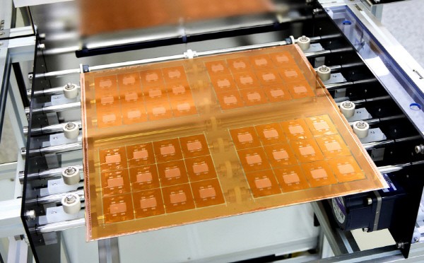
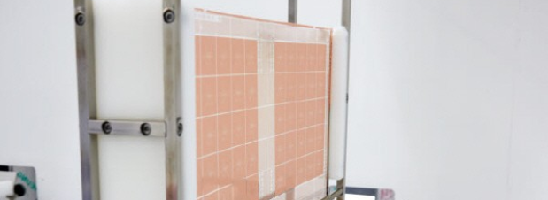
Grundlegendes zum Substrat für benutzerdefinierte Glasklassenpakete
Was sind Glassubstrate??
Glassubstrate sind dünn, starre Materialien aus hochreinem Glas, Entwickelt, um als Grundschicht in der Halbleiterverpackung zu dienen. Im Gegensatz zu herkömmlichen organischen oder silikonbasierten Substraten, Glas bietet hervorragende mechanische und elektrische Eigenschaften, Dies macht es zur bevorzugten Wahl für fortschrittliche Verpackungslösungen. Benutzerdefiniertes Glasklassenpaket-Substrat wurde speziell entwickelt, um die Leistung und Zuverlässigkeit von Halbleiterbauelementen der nächsten Generation zu verbessern. Es bietet eine stabile Plattform für hochdichte Verbindungen, entscheidend für Anwendungen in der KI, Hochleistungs-Computing, und 5G-Kommunikation.
Wichtige Materialeigenschaften von Glassubstraten
Die Vorteile von Benutzerdefiniertes Glasklassenpaket-Substrat resultieren aus den einzigartigen Materialeigenschaften:
- Geringer dielektrischer Verlust: Glas hat eine deutlich geringere Dielektrizitätskonstante (Dk) und Verlustfaktor (Df) im Vergleich zu organischen Substraten, Dies ermöglicht eine höhere Signalintegrität und reduziertes Übersprechen in Hochfrequenzanwendungen.
- Hohe thermische Stabilität: Mit ausgezeichneter thermischer Beständigkeit, Glassubstrate können extremen Temperaturen standhalten, Gewährleistung der Zuverlässigkeit in anspruchsvollen elektronischen Umgebungen.
- Überlegene mechanische Steifigkeit: Glas weist eine hohe Steifigkeit und einen geringen Verzug auf, Dies ist entscheidend für die Aufrechterhaltung der Dimensionsstabilität bei mehrschichtigen Halbleiterverpackungen.
Glassubstrat vs. Organisches Substrat: Vorteile und Einschränkungen
Während organische Substrate in der Halbleiterverpackung weit verbreitet sind, Benutzerdefiniertes Glasklassenpaket-Substrat bietet mehrere entscheidende Vorteile:
| Besonderheit | Glassubstrat | Organisches Substrat |
|---|---|---|
| Dielektrizitätskonstante | Untere, besser für Hochgeschwindigkeitssignale | Höher, was zu einem erhöhten Signalverlust führt |
| Thermische Stabilität | Exzellent, hält hohen Temperaturen stand | Beschränkt, anfällig für Wärmeausdehnung |
| Mechanische Stärke | Hohe Steifigkeit, minimaler Verzug | Geringere Steifigkeit, anfällig für Verformungen |
| Miniaturisierung | Ermöglicht eine feinere Tonhöhe und höhere Dichte | Begrenzt bei Anwendungen mit ultrafeiner Teilung |
| Herstellungskosten | Höher, aufgrund komplexer Verarbeitung | Untere, etablierter Produktionsprozess |
Die Rolle von kundenspezifischen Glasklassen-Paketsubstraten in der Halbleiterverpackung
Da Halbleitergeräte immer kleiner werden und gleichzeitig an Leistung gewinnen, Verpackungstechnologien müssen sich weiterentwickeln, um den höheren Anforderungen an die Signalintegrität gerecht zu werden, Energieeffizienz, und Wärmemanagement. Maßgeschneiderte Glasklasse Paketsubstrat revolutioniert Halbleiterverpackung indem es eine fortschrittliche Alternative zu herkömmlichen organischen Substraten bietet, Bereitstellung hervorragender elektrischer Eigenschaften, mechanische Stabilität, und thermische Leistung.
Glassubstrat für Verpackungen: Verbesserung der Signalintegrität und des Wärmemanagements
Einer der Hauptvorteile des Custom Glass Class Package Substrates ist seine Fähigkeit, die Signalintegrität deutlich zu verbessern. Mit einer niedrigeren Dielektrizitätskonstante (Dk) und minimaler dielektrischer Verlust (Df), Glassubstrate ermöglichen eine schnellere und zuverlässigere Datenübertragung, Damit sind sie ideal für Hochfrequenzanwendungen wie KI-Prozessoren, 5G-Netzwerke, und Hochleistungs-Computing (HPC). Zusätzlich, Glas weist eine hervorragende thermische Stabilität auf, Reduzierung von Verformungen und Verbesserung der Wärmeableitung. Dies ermöglicht ein besseres Wärmemanagement, Dies ist entscheidend, um eine Überhitzung in dicht gepackten Halbleiterbauelementen zu verhindern.
TSMC-Glassubstrat-Initiative: Integration von Glas in fortschrittliche Verpackungen
TSMC, ein führendes Unternehmen in der Halbleiterfertigung, hat sich aktiv mit der Custom Glass Class Package Substrate-Technologie beschäftigt, um die Grenzen der Chipleistung zu erweitern. Das Unternehmen integriert Glassubstrate in seine Roadmap für fortschrittliche Verpackungen, insbesondere für Chiplet-Architekturen und Speicher mit hoher Bandbreite (HBM) Anwendungen. Durch Nutzung der überlegenen elektrischen Isolierung und mechanischen Stabilität von Glas, Ziel von TSMC ist es, die Verbindungsdichte zu verbessern und gleichzeitig den Stromverbrauch zu senken, Ermöglicht Halbleiterlösungen der nächsten Generation.
Samsung & LG Innotek Glassubstratbemühungen: Innovationen und Fertigungskapazitäten
Auch Samsung und LG Innotek machen erhebliche Fortschritte bei der Entwicklung von Custom Glass Class Package Substraten. Samsung konzentriert sich auf großvolumige Produktionstechniken, die die Glasverarbeitung für fortschrittliche Halbleiterverpackungen optimieren, insbesondere bei KI-Beschleunigern und mobilen Prozessoren. In der Zwischenzeit, LG Innotek entwickelt innovative Fertigungsmethoden, um die Herstellbarkeit von Glassubstraten zu verbessern, Gewährleistung höherer Ausbeute und kosteneffektiver Produktion. Beide Unternehmen investieren stark in R&D, um ihre Glassubstrattechnologien zu verfeinern, positionieren sich als Hauptakteure beim Übergang von organischen zu glasbasierten Halbleiterverpackungen.
Glassubstrat vs. Organisches Substrat: Ein vergleichender Überblick
Während organische Substrate aufgrund ihrer geringeren Kosten und etablierten Herstellungsverfahren die Halbleiterverpackungsindustrie dominieren, Das kundenspezifische Glass Class Package-Substrat bietet klare Vorteile für Geräte der nächsten Generation:
| Besonderheit | Glassubstrat | Organisches Substrat |
|---|---|---|
| Signalintegrität | Hoch, aufgrund geringerer dielektrischer Verluste | Mäßig, bei höheren Frequenzen begrenzt |
| Wärmeleitfähigkeit | Exzellent, unterstützt eine bessere Wärmeableitung | Untere, die zusätzliche Kühllösungen erfordern |
| Mechanische Stabilität | Starr, minimaler Verzug | Anfällig für Ausdehnung und Verformung |
| Verbindungsdichte | Hoch, ermöglicht eine feinere Tonhöhe und Skalierung | Begrenzt durch Materialbeschränkungen |
| Kosten | Höher, aber mit der Massenproduktion besser | Untere, weit verbreitet in vorhandenen Verpackungen |
Glaskernsubstrat: Die nächste Verpackungsgeneration mit maßgeschneidertem Verpackungssubstrat der Glasklasse
Als Halbleitergeräte weiter voranschreiten, Herkömmliche Verpackungsmaterialien wie Silizium und organische Substrate stoßen an ihre physikalischen und elektrischen Grenzen. Um diese Herausforderungen zu meistern, Als innovative Lösung hat sich das kundenspezifische Glass Class Package-Substrat herausgestellt, mit Glaskernsubstraten, die bei der Halbleiterverpackung der nächsten Generation wegweisend sind. Durch die Nutzung der überlegenen Materialeigenschaften von Glas, Diese Technologie verändert das Hochleistungsrechnen, KI, und 5G-Anwendungen.
Was ist ein Glaskernsubstrat??
Ein Glaskernsubstrat ist eine Art fortschrittliches Halbleiterverpackungsmaterial, das Glas als zentrale Strukturschicht anstelle von organischen oder siliziumbasierten Materialien verwendet. Im Gegensatz zu herkömmlichen Substraten, die auf organischen Laminaten oder Siliziumwafern basieren, Glaskernsubstrate bieten eine einzigartige Kombination elektrischer Isolierung, mechanische Steifigkeit, und thermische Stabilität. Benutzerdefiniertes Glasklassenpaket-Substrat mit Glaskern ermöglicht feinere Verbindungsabstände, Verbesserte Signalintegrität, und verbesserte thermische Leistung, Dies macht es zur idealen Wahl für Chiplet-Architekturen und Speicher mit hoher Bandbreite (HBM) Integration.
Vorteile von Glaskernsubstraten gegenüber Silizium- und organischen Substraten
Im Vergleich zu herkömmlichen Verpackungsmaterialien, Benutzerdefiniertes Glasklassenpaket-Substrat mit Glaskern bietet mehrere wesentliche Vorteile:
| Besonderheit | Glaskernsubstrat | Siliziumsubstrat | Organisches Substrat |
|---|---|---|---|
| Elektrische Leistung | Geringer Verlust, bessere Signalintegrität | Hoher Verlust, höherer Stromverbrauch | Mäßig, aber bei hohen Frequenzen begrenzt |
| Wärmeausdehnung (CTE) | Passend zu Halbleitermaterialien, Stress reduzieren | Hoch, was zu potenziellen Zuverlässigkeitsproblemen führen kann | Höhere Ausdehnung, was zu Verwerfungen führt |
| Mechanische Steifigkeit | Hohe Steifigkeit, geringer Verzug | Spröde, anfällig für Risse | Flexibel, aber anfällig für Verformungen |
| Herstellungskosten | Mäßig, Verbesserung durch Massenproduktion | Hoch, aufgrund komplexer Verarbeitung | Niedrig, aber begrenzt für High-End-Anwendungen |
| Miniaturisierung | Ermöglicht feinere Verbindungen und eine höhere Dichte | Begrenzt durch mechanische Zerbrechlichkeit | Begrenzt durch Materialeigenschaften |
Die Kombination dieser Eigenschaften macht Benutzerdefiniertes Glasklassenpaket-Substrat mit Glaskern eine ausgezeichnete Wahl für Anwendungen, die eine Hochgeschwindigkeits-Datenübertragung erfordern, Miniaturisierung, und robuste Zuverlässigkeit.
Einführung von Glaskernsubstraten durch führende Halbleiterunternehmen
Erkennen der Vorteile von Benutzerdefiniertes Glasklassenpaket-Substrat, Große Halbleiterunternehmen investieren aktiv in die Glaskernsubstrattechnologie:
- TSMC entwickelt Glaskernsubstrate, um seine fortschrittlichen Verpackungslösungen zu verbessern, wie InFO und CoWoS, Dies ermöglicht eine höhere Verbindungsdichte für KI- und HPC-Chips.
- Intel hat bedeutende Fortschritte in der Glassubstratforschung angekündigt, Ziel ist es, die Glaskerntechnologie in seine Prozessoren der nächsten Generation zu integrieren, um die Energieeffizienz und die Wärmeleistung zu verbessern.
- Samsung erweitert seine Produktionskapazitäten für Glassubstrate, um der steigenden Nachfrage nach KI-Beschleunigern und 5G-Infrastruktur gerecht zu werden.
- LG Innotek verfeinert seine Fertigungstechniken für die Großserienfertigung, positioniert sich als wichtiger Lieferant im aufstrebenden Markt für Glassubstrate.
Da Branchenführer weiterhin die Grenzen der Halbleiterverpackung erweitern, Benutzerdefiniertes Glasklassenpaket-Substrat mit einem Glaskern wird voraussichtlich eine entscheidende Rolle in der nächsten Welle technologischer Fortschritte spielen. Mit kontinuierlichen Verbesserungen der Herstellungstechniken und Kostensenkungsstrategien, Glassubstrate sollen zum neuen Industriestandard für Hochleistungshalbleiteranwendungen werden.
Hauptvorteile des kundenspezifischen Glasklassenpaketsubstrats
Mit dem Fortschritt der Halbleitertechnologie, Verpackungslösungen müssen der steigenden Nachfrage nach höherer Leistung gerecht werden, größere Zuverlässigkeit, und verbesserte Miniaturisierung. Benutzerdefiniertes Glasklassenpaket-Substrat entwickelt sich aufgrund seiner einzigartigen Materialeigenschaften zu einer überlegenen Alternative zu herkömmlichen organischen und siliziumbasierten Substraten. Von verbesserter elektrischer Leistung bis hin zu überlegener mechanischer Festigkeit, Benutzerdefiniertes Glasklassenpaket-Substrat setzt einen neuen Standard für fortschrittliche Halbleiterverpackungen.
1. Elektrische Leistung: Geringerer Signalverlust, Bessere Impedanzkontrolle
Einer der Hauptvorteile von Benutzerdefiniertes Glasklassenpaket-Substrat sind seine außergewöhnlichen elektrischen Eigenschaften. Glas hat eine niedrigere Dielektrizitätskonstante (Dk) und dielektrischer Verlust (Df) im Vergleich zu organischen Substraten, Dadurch werden Signalverluste erheblich reduziert und die Hochfrequenzleistung verbessert. Dadurch sind Glassubstrate ideal für Anwendungen wie KI-Prozessoren, 5G-Netzwerke, und Hochleistungs-Computing (HPC), wo die Aufrechterhaltung der Signalintegrität von entscheidender Bedeutung ist. Zusätzlich, Benutzerdefiniertes Glasklassenpaket-Substrat ermöglicht eine präzisere Impedanzsteuerung, Minimierung der Signalverzerrung und Verbesserung der Gesamtleistungseffizienz in Halbleiterbauelementen.
2. Mechanische Stärke: Höhere Steifigkeit im Vergleich zu organischen Substraten
Mechanische Stabilität ist ein entscheidender Faktor bei der Halbleiterverpackung, da Verwerfungen und Verformungen die Leistung und Zuverlässigkeit des Geräts beeinträchtigen können. Benutzerdefiniertes Glasklassenpaket-Substrat bietet im Vergleich zu organischen Substraten eine höhere Steifigkeit und einen geringeren Verzug, Gewährleistung einer besseren strukturellen Integrität während der Herstellungs- und Betriebsphase. Im Gegensatz zu organischen Substraten, die sich unter hohen Temperaturen und mechanischer Belastung verformen können, Glassubstrate behalten ihre Form und Maßhaltigkeit, Dadurch eignen sie sich besser für fortschrittliche Verpackungstechnologien wie die Chiplet-Integration und 2,5D/3D-Stacking.
3. Thermalmanagement: Verbesserte Wärmeableitungseigenschaften
Die Wärmeableitung ist eine große Herausforderung bei Hochleistungshalbleiterbauelementen. Benutzerdefiniertes Glasklassenpaket-Substrat zeichnet sich durch hohe thermische Stabilität und effiziente Wärmeleitungseigenschaften im Wärmemanagement aus. Im Gegensatz zu organischen Substraten, die eine geringere Wärmeleitfähigkeit haben und möglicherweise zusätzliche Wärmeableitungslösungen erfordern, Glassubstrate unterstützen von Natur aus eine bessere Wärmeverteilung, Reduzierung von Hotspots und Verbesserung der Gesamtsystemzuverlässigkeit. Das macht Benutzerdefiniertes Glasklassenpaket-Substrat Besonders vorteilhaft für Hochleistungsanwendungen, einschließlich Rechenzentren, Automobilelektronik, und KI-Beschleuniger.
4. Miniaturisierung: Aktiviert Thinner, Kompaktere Designs für fortschrittliche Geräte
Der Trend bei der Halbleiterverpackung geht in Richtung zunehmender Miniaturisierung, Benutzerdefiniertes Glasklassenpaket-Substrat spielt eine entscheidende Rolle bei der Ermöglichung ultradünn, Designs mit hoher Dichte. Glassubstrate ermöglichen feinere Verbindungsabstände, höhere Routing-Dichten, und bessere Planarität, die für die Integration von mehr Komponenten auf kleinerem Raum unerlässlich sind. Im Vergleich zu organischen Substraten, Glas bietet eine hervorragende Oberflächenebenheit, Dies erhöht die Präzision fortschrittlicher Lithographieprozesse und ermöglicht kompaktere und energieeffizientere Halbleiterbauelemente. Dies ist insbesondere für mobile Prozessoren der nächsten Generation von Vorteil, tragbare Technologie, und ultrakompakte KI-Chips.
Glas vs. Siliziumsubstrat: Hauptunterschiede beim Substrat für kundenspezifische Glasklassenpakete
Während sich die Halbleiterverpackungstechnologie weiterentwickelt, Die Industrie sucht nach Alternativen zu herkömmlichen Siliziumsubstraten, um die Leistung zu verbessern, Kosten senken, und die Skalierbarkeit verbessern. Benutzerdefiniertes Glasklassenpaket-Substrat hat sich als vielversprechende Lösung herausgestellt, bietet im Hinblick auf die Fertigungseffizienz einzigartige Vorteile gegenüber Siliziumsubstraten, elektrische und thermische Eigenschaften, und Gesamtkosteneffizienz. In diesem Abschnitt werden die wichtigsten Unterschiede zwischen untersucht Benutzerdefiniertes Glasklassenpaket-Substrat und Siliziumsubstrate, Es wird hervorgehoben, warum Glas in modernen Halbleiterverpackungen an Bedeutung gewinnt.
1. Variationen im Herstellungsprozess
Die Herstellung von Benutzerdefiniertes Glasklassenpaket-Substrat unterscheidet sich deutlich von dem von Siliziumsubstraten. Siliziumbasierte Substrate werden typischerweise mithilfe von Wafer-Herstellungsprozessen hergestellt, die eine Hochtemperaturoxidation beinhalten, Doping, Photolithographie, und Radierung. Für diese Prozesse sind fortschrittliche Siliziumwafer in Halbleiterqualität erforderlich, deren Herstellung kostspielig und aufwändig ist.
Im Gegensatz, Benutzerdefiniertes Glasklassenpaket-Substrat nutzt bewährte Glasherstellungstechniken, einschließlich Präzisionsglasschneiden, chemische Stärkung, Microvia-Bohren, und Metallisierung. Glassubstrate können aus großen Glasplatten hergestellt werden, Dies ermöglicht eine höhere Ausbeute und eine kostengünstigere Produktion als Siliziumwafer. Zusätzlich, fortschrittliche Technologien wie Durchglasdurchkontaktierungen (TGV) ermöglichen hochdichte Verbindungen bei gleichzeitig hervorragender elektrischer Leistung.
| Besonderheit | Benutzerdefiniertes Glasklassenpaket-Substrat | Siliziumsubstrat |
|---|---|---|
| Grundmaterial | Hochreines Glas | Monokristallines Silizium |
| Herstellungsprozess | Panelbasiert, skalierbar | Waferbasiert, Komplex |
| Über Bildung | Durchglasdurchkontaktierungen (TGV) | Durchkontaktierungen durch Silizium (TSV) |
| Skalierbarkeit | Große Platten für die Massenproduktion | Begrenzt auf Wafergröße |
2. Vergleich der elektrischen und thermischen Eigenschaften
Benutzerdefiniertes Glasklassenpaket-Substrat bietet im Hinblick auf die elektrische Isolierung und die Wärmeausdehnungseigenschaften erhebliche Vorteile gegenüber Silizium. Silizium, ein Halbleiter sein, erfordert zusätzliche Isolationsschichten, um Kriechströme zu verhindern, wohingegen Glas von Natur aus ein ausgezeichneter elektrischer Isolator ist. Dies führt zu einer geringeren parasitären Kapazität und einer verbesserten Signalintegrität in Hochfrequenzanwendungen.
Ein weiterer kritischer Faktor ist die Wärmeausdehnung. Silizium hat einen hohen Wärmeausdehnungskoeffizienten (CTE) Nichtübereinstimmung mit Halbleiterchips, Dies kann zu mechanischer Belastung und Zuverlässigkeitsproblemen führen. Benutzerdefiniertes Glasklassenpaket-Substrat, Jedoch, hat einen CTE, der dem von Halbleitermaterialien näher kommt, Reduzierung von Stress und Verbesserung der langfristigen Zuverlässigkeit in Hochleistungsanwendungen.
| Eigentum | Benutzerdefiniertes Glasklassenpaket-Substrat | Siliziumsubstrat |
|---|---|---|
| Dielektrizitätskonstante | Untere (besser für die Signalintegrität) | Höher (erfordert eine zusätzliche Isolierung) |
| Elektrische Isolierung | Exzellent | Erfordert Oxidschichten |
| Wärmeausdehnung (CTE) | Passend zu Halbleitermaterialien | Nichtübereinstimmung mit Chips |
| Wärmeableitung | Mäßig | Hoch |
3. Kostenüberlegungen und Skalierbarkeit
Eine der größten Herausforderungen bei der Halbleiterverpackung besteht darin, Kosten und Skalierbarkeit in Einklang zu bringen. Während Siliziumsubstrate eine hervorragende Leistung bieten, Ihre Herstellung ist aufgrund der hohen Kosten von Siliziumwafern in Halbleiterqualität und der komplexen Herstellungsprozesse teuer. Im Gegensatz, Benutzerdefiniertes Glasklassenpaket-Substrat stellt aufgrund der geringeren Materialkosten und der Möglichkeit der Herstellung in großen Plattenformaten eine kostengünstigere Alternative dar, Verbesserung der Produktionseffizienz.
Skalierbarkeit ist ein weiterer wichtiger Vorteil von Benutzerdefiniertes Glasklassenpaket-Substrat. Glassubstrate können in größeren Panelgrößen hergestellt werden, Dies ermöglicht einen höheren Durchsatz und reduziert die Kosten pro Einheit. Dies macht Glas zu einer attraktiven Option für die Massenproduktion fortschrittlicher Halbleitergehäuse, inklusive Chiplets, Speicher mit hoher Bandbreite (HBM), und KI-Beschleuniger.
| Faktor | Benutzerdefiniertes Glasklassenpaket-Substrat | Siliziumsubstrat |
|---|---|---|
| Materialkosten | Untere (Glas ist reichlich vorhanden) | Höher (Siliziumwafer sind teuer) |
| Herstellungskosten | Untere (skalierbarer Panel-basierter Prozess) | Höher (Waferbasiert, komplexe Prozesse) |
| Skalierbarkeit | Hoch (große Panelgrößen) | Begrenzt auf Wafergröße |
Branchenakzeptanz & Zukünftige Trends bei kundenspezifischen Glasklassen-Paketsubstraten
Die Halbleiterindustrie durchläuft einen großen Wandel, da Unternehmen nach neuen Verpackungslösungen suchen, um die Leistung zu steigern, Reduzieren Sie den Stromverbrauch, und ermöglichen höhere Verbindungsdichten. Benutzerdefiniertes Glasklassenpaket-Substrat gewinnt als Alternative der nächsten Generation zu herkömmlichen Silizium- und organischen Substraten an Bedeutung, überlegene elektrische Leistung bieten, mechanische Stabilität, und Skalierbarkeit. Als Nachfrage nach Hochleistungsrechnen (HPC), künstliche Intelligenz (KI), und 5G-Technologien wachsen, Das sagen führende Halbleiterhersteller und Marktanalysten voraus Benutzerdefiniertes Glasklassenpaket-Substrat wird in der Zukunft der fortschrittlichen Verpackung eine entscheidende Rolle spielen.
Entwicklung von Intel-Glassubstraten: Ihr Ansatz und ihre Auswirkungen auf den Markt
Intel war an der Spitze Benutzerdefiniertes Glasklassenpaket-Substrat Forschung und Entwicklung, Ziel ist es, die Einschränkungen aktueller Verpackungsmaterialien zu überwinden. Das Unternehmen hat seine Fortschritte in der Glassubstrattechnologie öffentlich bekannt gegeben, Dies unterstreicht sein Potenzial, Multi-Chip-Packaging und Verbindungen mit hoher Dichte zu revolutionieren.
Der Ansatz von Intel konzentriert sich auf die Hebelwirkung Benutzerdefiniertes Glasklassenpaket-Substrat zu erreichen:
- Höhere Verbindungsdichte: Glas ermöglicht feinere Linienabstände und kleinere Durchgangsgrößen, entscheidend für fortschrittliche Chiplet-Architekturen.
- Bessere thermische Leistung: Eine verbesserte Wärmeableitung trägt dazu bei, den steigenden Strombedarf von KI-Beschleunigern und Hochleistungsprozessoren zu decken.
- Reduzierter Stromverbrauch: Ein geringerer dielektrischer Verlust führt zu einer verbesserten Signalintegrität, Reduzierung von Stromverlusten und Verbesserung der Effizienz.
Durch Integration Benutzerdefiniertes Glasklassenpaket-Substrat in seine Verpackungs-Roadmap ein, Intel möchte das Mooresche Gesetz erweitern, indem es höhere Transistordichten und effizientere Stromversorgungsnetzwerke ermöglicht. Das Unternehmen geht davon aus, dass Glassubstrate die Chipdesigns der nächsten Generation grundlegend verändern werden, insbesondere bei leistungsstarken Serverprozessoren und KI-Chips.
Einblicke in die Yole-Gruppe: Markttrends und Wettbewerb zwischen Verpackungsriesen
Das Marktforschungsunternehmen Yole Group hat die Entwicklung genau beobachtet Benutzerdefiniertes Glasklassenpaket-Substrat, unter Hinweis auf steigende Investitionen von großen Playern wie TSMC, Samsung, LG Innotek, und ASE-Gruppe. Laut Yoles neuesten Berichten, Die Nachfrage nach Glassubstraten in der Halbleiterverpackung wird durch den Bedarf an getrieben:
- Hochfrequenzanwendungen: KI, 5G, und Hochgeschwindigkeitsrechnen erfordern Substrate mit geringerem Signalverlust und besserer Impedanzkontrolle.
- Miniaturisierungstrends: Glassubstrate ermöglichen eine dünnere Ausführung, kompaktere Verpackungslösungen, unverzichtbar für mobile und tragbare Geräte.
- Fortschrittliche Multi-Chip-Verpackung: Da Chiplet-basierte Architekturen immer beliebter werden, Glassubstrate bieten bessere Routing-Fähigkeiten und reduziertes Übersprechen.
Der Wettbewerb zwischen führenden Verpackungsriesen verschärft sich, mit Unternehmen, die um die Kommerzialisierung wetteifern Benutzerdefiniertes Glasklassenpaket-Substrat Technologie. Während Intel und TSMC bei R führend sind&D, Samsung und LG Innotek investieren stark in die Massenproduktionskapazitäten, mit dem Ziel, sich als wichtiger Anbieter auf dem Glassubstratmarkt zu etablieren.
Zukunftsausblick: Masseneinführung in 2,5D- und 3D-Verpackungen
Die Zukunft von Benutzerdefiniertes Glasklassenpaket-Substrat ist eng mit der Entwicklung der 2,5D- und 3D-Verpackung verbunden. Glassubstrate bieten mehrere Vorteile, die sie ideal für diese fortschrittlichen Verpackungstechniken machen:
- 2.5D-Integration: Glassubstrate ermöglichen hochdichte Interposer mit überlegener elektrischer Leistung im Vergleich zu Alternativen auf Siliziumbasis.
- 3D Stapeln: Ihr geringer Wärmeausdehnungskoeffizient (CTE) reduziert die Spannung zwischen gestapelten Matrizen, Verbesserung der Zuverlässigkeit und Langlebigkeit.
- Verpackung auf Panelebene (PLP): Die Möglichkeit, Glassubstrate in großen Panels herzustellen, verbessert die Produktionseffizienz, Senkung der Kosten für die Masseneinführung.
Mit ständigen Fortschritten in der Fertigungstechnologie, Benutzerdefiniertes Glasklassenpaket-Substrat wird voraussichtlich eine Mainstream-Lösung für Halbleiterbauelemente der nächsten Generation werden. Da große Halbleiterunternehmen weiterhin innovativ sind, Glassubstrate werden wahrscheinlich herkömmliche Materialien im Hochleistungsrechnen ersetzen, KI-Prozessoren, und Netzwerkinfrastruktur, Wir gestalten die Zukunft der Halbleiterverpackung.