CO., LTD")
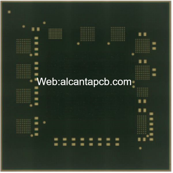
Substrat d'emballage FCBGA: Pas de bosse optimal de 100 µm, 9um trace et espace pour un design compact. Typique: 15-30euh trace et espacement.
Le substrat d'emballage FCBGA est une technologie innovante qui joue un rôle essentiel dans l'ingénierie des circuits imprimés.. Son nom complet est Flip-Chip Ball Grid Array. (Retourner la puce Ball Ball Grid Bread) substrat d'emballage, spécialement conçu pour répondre aux exigences de performance et de fiabilité des circuits intégrés (CI). En tant que composant clé des équipements électroniques, Le substrat d'emballage FCBGA joue un rôle de pont entre la puce et la carte de circuit imprimé (PCB).
La conception du substrat d'emballage FCBGA prend en compte les besoins particuliers des puces de circuits intégrés et s'engage à fournir des connexions électriques optimales., gestion thermique et support mécanique. L'introduction de cette technologie de substrat fournit une base solide pour l'amélioration des performances et l'assurance de la fiabilité des équipements électroniques.. Les principales caractéristiques des substrats d'emballage FCBGA et leur importance dans l'ingénierie des circuits imprimés seront discutées en détail ci-dessous..
Dans l’évolution de l’ingénierie des circuits imprimés, l'introduction du substrat de conditionnement FCBGA marque une percée innovante dans le domaine du conditionnement de circuits intégrés. Cette technologie est spécialement conçue pour relever les défis rencontrés par les méthodes d'emballage traditionnelles face aux puces hautes performances., en particulier dans des domaines tels que la transmission du signal, gestion thermique et densité d'emballage.
Prise en charge des performances et de la fiabilité des circuits intégrés
L'objectif principal du Substrat d'emballage FCBGA est de fournir un support complet au circuit intégré pour garantir qu'il puisse atteindre des niveaux de performances et de fiabilité optimaux pendant le fonctionnement. En assurant des connexions électriques précises, le substrat réduit efficacement les pertes de transmission du signal et aide à maintenir la stabilité de la transmission de données à grande vitesse.
Un rôle de pont important
Comme pont entre la puce et le PCB, le substrat d'emballage FCBGA occupe une position clé dans l'ensemble du système de circuit. Ce n'est pas seulement un support pour connecter des puces, mais entreprend également la tâche de transmettre de l'énergie électrique et des signaux de données. En outre, la conception de gestion thermique du substrat aide à maintenir la température de fonctionnement appropriée de la puce et améliore la fiabilité de l'ensemble du système.
composants clés
Lors de la conception d'appareils électroniques complexes, les ingénieurs considèrent souvent les substrats d'emballage FCBGA comme un composant clé indispensable. Sa structure et ses performances affectent directement la stabilité et les performances du produit final. Donc, le choix de cette technologie de substrat devient une décision clé pour garantir un fonctionnement fiable à long terme de l'équipement.
Dans l'ensemble, la nouvelle application des substrats de conditionnement FCBGA dans l'ingénierie des cartes de circuits imprimés démontre sa contribution exceptionnelle à la performance et à la fiabilité des circuits intégrés. Cette technologie de substrat spécialement conçue n'est pas seulement une innovation technologique dans les équipements électroniques, mais aussi une garantie importante pour garantir que les puces hautes performances peuvent fonctionner de manière stable dans divers scénarios d'application.
Quelle est la fonction du substrat d'emballage FCBGA?
Substrat d'emballage FCBGA, comme l'une des technologies clés de l'ingénierie des circuits, joue un rôle indispensable dans la connexion des puces de circuits intégrés (IC) et cartes de circuits imprimés (PCB). Sa tâche principale est de devenir un pont entre les deux et d'assurer la meilleure connexion électrique, gestion thermique et support mécanique du circuit intégré pour assurer un fonctionnement efficace et stable de l'ensemble du système.
Connexion électrique: le lien entre les signaux
Dans les appareils électroniques modernes, la complexité des circuits intégrés augmente de jour en jour, et le substrat du boîtier FCBGA fournit des connexions électriques supérieures grâce à sa conception et sa disposition uniques. À travers la structure du Ball Grid Array, le substrat d'emballage FCBGA relie les broches de la puce aux points correspondants du PCB. Cette méthode de connexion sophistiquée permet non seulement d'obtenir une interconnexion électrique haute densité, mais offre également une excellente intégrité du signal, jeter des bases solides pour le fonctionnement normal du CI.
Gestion thermique: La clé d'un refroidissement efficace
À mesure que les performances des appareils électroniques s'améliorent, la chaleur générée par les circuits intégrés devient de plus en plus importante. Le substrat d'emballage FCBGA gère et disperse efficacement la chaleur générée par la puce grâce à une structure de dissipation thermique soigneusement conçue.. Cela permet non seulement de maintenir la température de fonctionnement du circuit intégré dans une plage sûre., mais assure également la stabilité et la fiabilité de l'ensemble du système. L'application de matériaux thermoconducteurs et la conception intelligente de dissipation thermique font des substrats d'emballage FCBGA un choix idéal pour les appareils électroniques hautes performances..
Support mécanique: une base solide et solide
Les appareils électroniques sont souvent affectés par des forces externes telles que les vibrations et les impacts., et les substrats d'emballage FCBGA jouent un rôle clé dans ce domaine. Sa structure fournit non seulement un bon support mécanique au circuit intégré et empêche le déplacement ou l'endommagement de la puce pendant le transport et l'utilisation., mais est également capable de s'adapter aux contraintes mécaniques dans divers environnements de travail pour assurer la stabilité et la durabilité de l'ensemble du système.
Dans l'ensemble, Le substrat d'emballage FCBGA n'est pas seulement un pont entre IC et PCB, mais aussi un représentant du savoir-faire exquis qui relie, gère et prend en charge les composants électroniques dans le monde électronique moderne. Grâce à d'excellentes connexions électriques, gestion thermique efficace et support mécanique fiable, Les substrats d'emballage FCBGA garantissent que les circuits intégrés peuvent fonctionner de manière optimale, offrant des performances et une fiabilité élevées à nos appareils électroniques. Dans cette ère technologique en évolution rapide, Les substrats d'emballage FCBGA sont à la pointe de l'ingénierie électronique, jeter des bases solides pour l’innovation et le développement.
Quels types de substrats d'emballage FCBGA existe-t-il?
En tant que technologie importante dans le domaine de l'ingénierie des PCB, Les substrats d'emballage FCBGA ont développé différents types pour différentes applications et besoins.. Ces types sont personnalisés en fonction d'exigences spécifiques et impliquent de nombreux aspects tels que les matériaux, configurations de couches et processus de fabrication. Donner une riche diversité à la technologie FCBGA.
Plusieurs choix de matériaux
La sélection des matériaux du substrat d'emballage FCBGA est la principale manifestation de la diversité. Différents scénarios d'application et exigences techniques peuvent conduire à des exigences différentes en matière de matériaux de substrat. Par exemple, certaines applications peuvent rechercher des matériaux de substrat à haute conductivité thermique, tandis que d'autres peuvent se concentrer davantage sur la résistance mécanique et la durabilité. Cette différence a conduit à la sélection de différents matériaux de substrat dans la technologie FCBGA, y compris, mais sans s'y limiter, FR-4, polyimide (PI), polyétheréthercétone (COUP D'OEIL), etc..
Combinaison flexible de configurations multi-niveaux
La diversité des substrats d'emballage FCBGA se reflète également dans la combinaison flexible de ses configurations de couches.. Différentes applications ont des exigences de circuit différentes, les substrats des boîtiers FCBGA peuvent donc utiliser différents nombres et dispositions de couches pour répondre à ces exigences.. La technologie FCBGA haut de gamme implique souvent des configurations de couches à plusieurs niveaux pour obtenir des connexions de circuits plus complexes et plus denses., améliorant ainsi les performances globales.
Innovation différenciée dans les processus de fabrication
Dans le développement de la technologie FCBGA, l’innovation différenciée dans les processus de fabrication est un maillon clé. L'évolution continue des diverses technologies de fabrication a permis aux substrats d'emballage FCBGA d'avoir une plus grande précision et une plus grande contrôlabilité pendant le processus de production.. L'introduction de technologies émergentes telles que la technologie de fabrication HDI améliorée et les méthodes semi-additifs ont encore amélioré l'efficacité de la production et la qualité des substrats d'emballage FCBGA..
Plus particulièrement, La diversité des substrats du boîtier FCBGA est obtenue grâce à des conceptions personnalisées spécifiques à l'application. Différentes industries et différentes demandes de produits ont conduit à la segmentation de la technologie FCBGA. Par exemple, le domaine des communications peut nécessiter des substrats d'emballage FCBGA qui se concentrent davantage sur les caractéristiques de transmission haute fréquence, tandis que l'électronique médicale pourrait se concentrer davantage sur la biocompatibilité et la stabilité.
Dans l'ensemble, la diversité des substrats d'emballage FCBGA n'est pas seulement le reflet de la technologie, mais aussi sa flexibilité pour répondre aux besoins des différents domaines. Cette diversité donne une impulsion au développement continu de la technologie FCBGA, lui permettant de s’adapter à l’évolution du marché et des environnements technologiques.
À l'avenir, avec l’émergence continue de nouveaux matériaux et de nouveaux procédés, et la recherche continue d'appareils électroniques hautes performances dans diverses industries, la diversité des substrats d'emballage FCBGA continuera à jouer un rôle clé dans la promotion de l'innovation en ingénierie des PCB.
Quelle est la différence entre le substrat d'emballage FCBGA et le PCB?
Dans le domaine de l'ingénierie PCB, bien que les substrats d'emballage FCBGA et les cartes de circuits imprimés traditionnelles (PCBS) j'ai des choses en commun, ils présentent des différences significatives dans leur structure et leur fonction. Le substrat d'emballage FCBGA est une technologie spécialement conçue pour répondre aux exigences uniques des circuits intégrés, miser sur la compacité, intégrité du signal et efficacité thermique.
Substrat de boîtier FCBGA vs. PWB et PCB
Cartes de câblage imprimées traditionnelles (PWB) et les PCB jouent un rôle fondamental dans les composants électroniques, tandis que le substrat d'emballage FCBGA est une forme spéciale conçue pour les circuits intégrés. Comparé aux PCB à usage général, Les substrats de conditionnement FCBGA accordent davantage d'attention à la satisfaction des besoins des circuits intégrés en matière de configuration compacte et de connexions hautes performances..
Substrat de boîtier FCBGA vs. carte mère
En général, la carte mère est une plate-forme complète qui intègre diverses technologies PCB, tandis que le substrat d'emballage FCBGA vise à fournir une plate-forme de support stable pour les circuits intégrés individuels.. Une carte mère peut contenir une variété de composants électroniques et de connexions, tandis que le substrat du boîtier FCBGA est spécialement conçu pour fournir une base fiable pour les circuits intégrés indépendants.
Substrat de boîtier FCBGA vs. substrat
Les substrats d'emballage FCBGA peuvent être considérés comme un sous-ensemble de substrats conçus pour répondre aux besoins uniques de la technologie des puces retournées.. Par rapport aux substrats à usage général, Les substrats d'emballage FCBGA accordent plus d'attention à la disposition et au câblage des circuits pour s'adapter aux exigences particulières de l'emballage des puces..
Substrat de boîtier FCBGA vs. PCB de type substrat (Orthophoniste)
Il peut y avoir des similitudes avec les PCB de type substrat (Orthophoniste), mais le substrat d'emballage FCBGA se concentre sur l'emballage des puces, mettant l'accent sur la compacité et la haute intégration des circuits. SLP pourrait être une technologie de carte de circuit imprimé flexible, mais ses objectifs de conception et son orientation sont différents de ceux des substrats d'emballage FCBGA.
Substrat de boîtier FCBGA vs. Substrat HDI
Interconnexion haute densité (HDI) les substrats font partie de la technologie PCB, mais au sein de la famille FCBGA, Les substrats HDI soulignent la nécessité d'un format compact, connexions performantes. Le substrat d'emballage FCBGA est conçu par des professionnels pour garantir le haut degré d'intégration et les connexions fiables nécessaires pour s'adapter à la technologie des puces retournées..
En résumé, le substrat d'emballage FCBGA répond aux besoins uniques des circuits intégrés en matière de performances, compacité et efficacité thermique grâce à sa structure et ses fonctions spécialement conçues. Cette technologie, qui se concentre sur l'emballage des puces, fournit un support essentiel pour la fiabilité et les performances des appareils électroniques.
Quelles sont les principales structures et technologies de production des substrats d'emballage FCBGA?
Substrat de boîtier FCBGA (Réseau de grilles à billes Flip-Chip) est un élément clé de l'ingénierie moderne des circuits imprimés. Sa structure et sa technologie de production ont été soigneusement conçues et continuellement innovées pour répondre aux besoins des circuits intégrés très complexes. (CI). Ce qui suit est une analyse détaillée de la structure principale et de la technologie de production du substrat d'emballage FCBGA.:
La conception structurelle du substrat d'emballage FCBGA prend en compte plusieurs facteurs, parmi lesquels l'intégrité du signal, la conduction thermique et le support mécanique sont cruciaux.
Intégrité du signal: La configuration d'empilement dans la structure est conçue pour maintenir au maximum l'intégrité du signal, garantissant une atténuation et un retard réduits du signal pendant la transmission haute fréquence.
Conduction thermique: La sélection de matériaux spéciaux et la disposition structurelle aident à optimiser la conduction thermique, assurer une température de fonctionnement stable à l’intérieur de la puce, et éviter les dommages dus à la surchauffe.
Support mécanique: La structure doit fournir un support mécanique suffisant pour éviter les effets néfastes des vibrations externes et des contraintes mécaniques sur le boîtier FCBGA et garantir une fiabilité à long terme..
Avec le développement continu de la technologie, la technologie de fabrication des substrats d'emballage FCBGA innove et évolue également constamment. Les technologies clés impliquées sont les suivantes:
Améliorations de la technologie de fabrication HDI: Interconnexion haute densité (HDI) la technologie joue un rôle clé dans la fabrication de substrats d’emballage FCBGA. Grâce à une technologie de fabrication HDI améliorée, plus de connexions peuvent être réalisées dans un espace limité et l'intégration des circuits imprimés peut être améliorée.
Incorporation de méthodes semi-additifs: La méthode semi-additif est une technique qui ajoute progressivement des couches de métal au cours du processus de fabrication.. L'application de cette méthode permet un contrôle plus précis de la répartition des métaux, améliorant la conductivité électrique et améliorant ainsi les performances globales.
Améliorations des performances et de la fiabilité
L'intégration de ces technologies de fabrication avancées améliore non seulement les performances globales du substrat d'emballage FCBGA., mais améliore également sa fiabilité. Avec une meilleure intégrité du signal, conduction thermique et support mécanique, Les substrats du boîtier FCBGA peuvent maintenir un fonctionnement stable dans des conditions de fonctionnement extrêmes.
Tendances et défis futurs
Bien que la technologie actuelle des substrats d'emballage FCBGA soit très avancée, avec le développement continu de la technologie électronique, il y a encore des défis constants et de nouvelles tendances. Les futures orientations de recherche pourraient inclure l’innovation matérielle, des interconnexions à plus haute densité et des processus de fabrication plus sophistiqués pour répondre aux demandes croissantes de performances des appareils électroniques.
Pris ensemble, l'innovation continue de la structure et de la technologie de fabrication des substrats d'emballage FCBGA a apporté des possibilités sans précédent au domaine de l'ingénierie des circuits imprimés. L'avancement continu de cette technologie favorisera l'amélioration des performances et la fiabilité des équipements électroniques et aidera la technologie future à continuer d'avancer..
FAQ sur les substrats du boîtier FCBGA
Comment les substrats de boîtier FCBGA peuvent-ils améliorer la gestion thermique?
Le substrat d'emballage FCBGA utilise une technologie et des matériaux avancés en matière de gestion thermique. D'abord, grâce à une structure soigneusement conçue, il peut conduire et disperser efficacement la chaleur générée par les circuits intégrés. En outre, matériaux avec une excellente conductivité thermique, tels que les couches métalliques et les supports de dissipation thermique, sont utilisés pour garantir le maintien de températures stables dans les applications hautes performances. Cela permet au substrat d'emballage FCBGA de maintenir une température contrôlable tout en maintenant le fonctionnement efficace à long terme du circuit intégré..
Le substrat d’emballage FCBGA peut-il être utilisé dans les produits électroniques grand public?
Fcbga (Réseau de grilles à billes Flip-Chip) les substrats d'emballage sont largement utilisés dans divers produits électroniques grand public, grâce à leur conception compacte et à leurs performances élevées. Cette technologie constitue une solution fiable et efficace pour une gamme d'appareils, y compris les téléphones portables, comprimés, caméras, et plus. La combinaison convaincante de performances électriques supérieures et d'efficacité spatiale positionne FCBGA comme le choix préféré dans l'industrie électronique grand public contemporaine..
Les avantages distincts des substrats d'emballage FCBGA, en particulier dans les domaines de la gestion thermique et des applications, soulignent leur rôle essentiel dans le respect des exigences strictes en matière de hautes performances et de stabilité des appareils électroniques. Répondre à ces préoccupations met non seulement en évidence l’efficacité de la technologie, mais approfondit également notre compréhension de la façon dont les substrats d’emballage FCBGA continuent de jouer un rôle central dans le paysage en évolution de l’électronique.. Dans une industrie mettant de plus en plus l’accent sur la miniaturisation et la haute performance, Les substrats d’emballage FCBGA sont prêts à conserver leur rôle central.
En plus des deux questions ci-dessus, il existe d'autres questions courantes pouvant impliquer le processus de fabrication des substrats d'emballage FCBGA, comparaison avec d'autres technologies d'emballage, etc.. Les réponses à ces questions aideront les lecteurs à avoir une compréhension plus complète du statut et de l'application des substrats d'emballage FCBGA dans l'ingénierie électronique moderne.. Avec le développement continu de la technologie, Les substrats d'emballage FCBGA continueront de promouvoir les performances et la fiabilité des équipements électroniques.