CO., LTD")
Fabricant de substrat de réseau de grille de boule de puce de Flip. En tant que leader Retourner la puce Fabricant de substrats à grille à billes, Nous nous spécialisons dans la production de substrats de haute performance pour des applications électroniques avancées. Nos processus de fabrication de pointe assurent une qualité et une fiabilité supérieures, Répondre aux demandes des industries telles que les télécommunications, calcul, et l'automobile. En tirant parti d’une technologie de pointe et d’un design innovant, nous fournissons des solutions qui améliorent les performances des appareils, soutenir la miniaturisation, et garantir une intégrité thermique et du signal robuste.
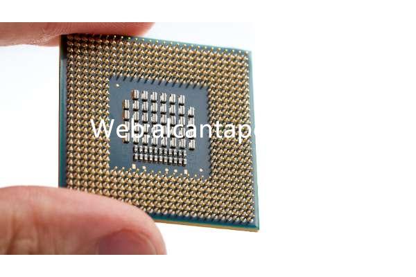
Le réseau de grilles Flip Chip Ball (FC-BGA) substrat est un composant essentiel de l'emballage électronique moderne, offrant une solution robuste pour les applications hautes performances et haute densité. Les substrats FC-BGA sont conçus pour prendre en charge les puces semi-conductrices avancées, assurer les connexions électriques, support mécanique, et dissipation de la chaleur. Ces substrats jouent un rôle central dans l'amélioration des performances et de la fiabilité des circuits intégrés (CI) dans diverses applications, allant de l'électronique grand public aux systèmes automobiles. Dans cet article, nous approfondirons les subtilités des substrats FC-BGA, explorer leur structure, matériels, processus de fabrication, domaines d'application, et avantages.
Qu'est-ce qu'un substrat FC-BGA?
Un substrat FC-BGA est un type de technologie d'emballage utilisé pour monter des puces semi-conductrices directement sur un substrat avec des bosses de soudure.. Contrairement au câblage filaire traditionnel, La technologie Flip Chip retourne la puce à l'envers, permettre à la zone active de faire face au substrat. Cette méthode offre plusieurs avantages, y compris des interconnexions à plus haute densité, performances électriques améliorées, et une meilleure gestion thermique.
Le substrat FC-BGA est constitué de plusieurs couches, comprenant une couche centrale, couches de construction, et couches de masque de soudure. La couche centrale est généralement constituée de matériaux comme le bismaléimide-triazine (Bt) résine ou époxy, qui offrent une excellente stabilité thermique et résistance mécanique. Couches de construction, en matériaux diélectriques et cuivre, sont ajoutés pour créer le câblage complexe requis pour les interconnexions haute densité. Les couches de masque de soudure protègent les circuits et empêchent les ponts de soudure pendant l'assemblage..
Les interconnexions entre la puce et le substrat sont réalisées à l'aide de bosses de soudure, qui sont de petites sphères de matériau de soudure placées sur les plages d'E/S de la puce. Pendant le montage, la puce est retournée et alignée avec le substrat, et les bosses de soudure sont refondues pour créer une connexion mécanique et électrique robuste. Ce processus permet un nombre plus élevé d'interconnexions par unité de surface par rapport au câblage filaire traditionnel..
Structure des substrats FC-BGA
The structure of FC-BGA substrates is complex and highly engineered to meet the demands of advanced semiconductor packaging. Les substrats sont généralement constitués de plusieurs composants clés:
The core layer provides the mechanical backbone of the substrate. Materials like BT resin or epoxy are commonly used due to their excellent thermal and mechanical properties. The core layer is typically rigid, offering stability and support for the entire substrate structure.
Multiple build-up layers are added on both sides of the core layer to create the necessary routing for electrical signals. These layers are made of dielectric materials, comme le cuivre recouvert de résine (RCC) ou époxy, and are interspersed with copper traces. The build-up layers enable the high-density wiring required for advanced ICs, allowing for intricate routing and multiple layers of interconnections.
Solder mask layers are applied on top of the build-up layers to protect the circuitry and prevent solder bridging. These layers are made of insulating materials and are crucial for maintaining the integrity of the electrical connections during assembly and operation.
Solder bumps are small spheres of solder material placed on the chip’s I/O pads. These bumps create the electrical and mechanical connection between the chip and the substrate. The solder bumps are typically made of lead-free solder materials, comme l'étain-argent-cuivre (SAC) alliages, to comply with environmental regulations.
The overall structure of an FC-BGA substrate is designed to optimize electrical performance, gestion thermique, et stabilité mécanique. The combination of core layers, couches de construction, solder mask layers, and solder bumps ensures reliable operation in demanding applications.
Matériaux utilisés dans les substrats FC-BGA
The materials used in FC-BGA substrates are carefully selected to meet the stringent requirements of high-performance semiconductor packaging. Les matériaux clés comprennent:
La couche centrale est généralement constituée de résine BT ou d'époxy. BT resin is favored for its excellent thermal stability, faible constante diélectrique, and good mechanical strength. Epoxy materials are also used for their cost-effectiveness and adequate performance in many applications.
The build-up layers use dielectric materials such as RCC or epoxy to insulate the copper traces and provide structural integrity. RCC materials are known for their low thermal expansion and high reliability, ce qui les rend adaptés aux interconnexions haute densité.
Copper is used extensively for the conductive traces in the build-up layers. It offers excellent electrical conductivity, conductivité thermique, et la fiabilité. The copper layers are typically formed through electroplating processes, allowing for precise control of trace dimensions and thickness.
The solder mask layers are made of insulating materials that protect the underlying circuitry and prevent solder bridging. These materials are typically epoxy-based and are applied using screen printing or photo-imaging techniques.
Les bosses de soudure sont constituées de matériaux de soudure sans plomb, such as SAC alloys. These materials offer good mechanical properties, excellent thermal fatigue resistance, and compliance with environmental regulations.
The careful selection and combination of these materials are crucial for achieving the desired electrical, thermique, and mechanical performance of FC-BGA substrates. Each material contributes to the overall reliability and performance of the substrate, ensuring that it meets the demands of advanced semiconductor packaging.
The Manufacturing Process of FC-BGA Substrates
The manufacturing process of FC-BGA substrates involves several intricate steps, each contributing to the overall quality and performance of the final product. Le processus comprend:
The first step involves preparing the core materials, matériaux diélectriques, et feuilles de cuivre. The core materials are typically laminated with copper foils to form the initial substrate.
Pour substrats multicouches, plusieurs couches de diélectrique et de cuivre sont empilées et liées ensemble à l'aide de processus de stratification. Cette étape nécessite un alignement et un contrôle précis pour garantir un enregistrement et une liaison appropriés de chaque couche..
After layer stacking, holes are drilled into the substrate to create vias and through-holes. Techniques de forage avancées, comme le perçage au laser, peut être utilisé pour les microvias et les exigences de haute précision. Les trous percés sont ensuite nettoyés et préparés pour le placage.
Les trous percés sont plaqués de cuivre pour créer des connexions électriques entre les couches. Cela implique de déposer une fine couche de cuivre sur les parois des trous grâce à des procédés de galvanoplastie.. Le processus de placage doit être soigneusement contrôlé pour garantir une couverture et une adhérence uniformes..
Les motifs de circuits souhaités sont transférés sur les couches de cuivre à l'aide d'un processus photolithographique.. Il s'agit d'appliquer un film photosensible (photorésist) à la surface du cuivre et en l'exposant aux ultraviolets (UV) Lumière à travers un photomasque. Les zones exposées de la résine photosensible sont développées, laisser derrière lui le modèle de circuit. La carte est ensuite gravée pour éliminer le cuivre indésirable, ne laissant que les traces du circuit.
Un masque de soudure est appliqué sur la carte pour protéger les circuits et empêcher les ponts de soudure. Le masque de soudure est généralement appliqué à l'aide de techniques de sérigraphie ou de photo-imagerie, puis durci pour le durcir..
Une finition de surface est appliquée sur les zones de cuivre exposées pour améliorer la soudabilité et protéger contre l'oxydation.. Les finitions de surface courantes incluent l'or à immersion au nickel autocatalytique (Accepter), Nivellement de la soudure à air chaud (Saigner), et argent d'immersion.
Des bosses de soudure sont placées sur les plots d'E/S de la puce, et la puce est ensuite retournée et alignée avec le substrat. Les bosses de soudure sont refondues pour créer une connexion mécanique et électrique robuste entre la puce et le substrat.
La dernière étape implique des tests et une inspection rigoureux pour garantir que le substrat répond à toutes les exigences de performance et de fiabilité.. Tests électriques, inspection visuelle, et inspection optique automatisée (AOI) sont utilisés pour identifier tout défaut ou irrégularité. Tous les problèmes identifiés lors des tests sont résolus avant que les substrats ne soient approuvés pour l'expédition..
The manufacturing process of FC-BGA substrates requires precise control and expertise to ensure high quality and reliability. Chaque étape est essentielle pour atteindre les performances et la fiabilité souhaitées du produit final..
Domaines d'application des substrats FC-BGA
FC-BGA substrates are used in a wide range of applications across various industries due to their high performance and reliability. Les principaux domaines d'application comprennent:
FC-BGA substrates are widely used in consumer electronics, comme les smartphones, comprimés, et consoles de jeu. These devices require high-performance ICs with advanced packaging solutions to achieve the desired performance and form factor. FC-BGA substrates provide the necessary interconnections, gestion thermique, and mechanical support for these high-performance chips.
L'industrie automobile s'appuie sur une électronique de pointe pour diverses applications, y compris les unités de commande du moteur (COUVERTURE), systèmes avancés d'aide à la conduite (ADAS), et systèmes d'infodivertissement. FC-BGA substrates offer the high reliability, gestion thermique, et stabilité mécanique requises pour les applications automobiles, assurer le fonctionnement sûr et efficace des systèmes électroniques des véhicules.
En télécommunications, FC-BGA substrates are used in base stations, infrastructure réseau, et dispositifs de communication. The high-density interconnections and superior electrical performance of FC-BGA substrates make them ideal for handling the high-frequency signals and data rates required in modern communication systems.
Dispositifs médicaux, tels que les systèmes d'imagerie, équipement de diagnostic, et dispositifs de surveillance des patients, nécessitent des circuits intégrés performants et fiables. FC-BGA substrates provide the necessary electrical performance, gestion thermique, et fiabilité pour ces applications critiques, garantir un fonctionnement précis et cohérent des dispositifs médicaux.
En électronique industrielle, FC-BGA substrates are used in automation systems, gestion de l'énergie, et systèmes de contrôle. Ces applications nécessitent des solutions d'emballage robustes et fiables pour résister à des conditions environnementales difficiles et garantir un fonctionnement continu.. FC-BGA substrates offer the necessary performance and durability for industrial applications.
Les applications aérospatiales et de défense exigent des systèmes électroniques de haute fiabilité et de hautes performances. FC-BGA substrates are used in radar systems, équipement de communication, et avionique, fournir les performances électriques nécessaires, gestion thermique, et stabilité mécanique pour les applications critiques.
Avantages des substrats FC-BGA
FC-BGA substrates offer several advantages that make them a preferred choice for high-performance and high-reliability applications. Ces avantages comprennent:
FC-BGA substrates enable a high number of interconnections per unit area, permettant des conceptions de circuits intégrés plus complexes et plus performantes. Cette haute densité est obtenue grâce à l'utilisation de bosses de soudure et de structures multicouches avancées., offrant des performances électriques et une intégrité du signal supérieures.
La technologie Flip Chip utilisée dans les substrats FC-BGA offre des chemins de signal plus courts et plus directs par rapport à la liaison filaire traditionnelle.. Cela entraîne une perte de signal plus faible, inductance et capacité parasites réduites, et une intégrité du signal améliorée, ce qui rend les substrats FC-BGA idéaux pour les applications haute fréquence et haute vitesse.
Les substrats FC-BGA offrent une gestion thermique efficace grâce à l'utilisation de matériaux à haute conductivité thermique et de structures optimisées. La configuration de la puce retournée permet également une dissipation directe de la chaleur de la puce vers le substrat., réduisant la résistance thermique et améliorant la dissipation thermique. Ceci est crucial pour les applications haute puissance où une gestion thermique efficace est essentielle pour un fonctionnement fiable..
The robust structure of FC-BGA substrates, y compris l'utilisation de résine BT ou de matériaux de base époxy, offre une excellente stabilité mécanique et fiabilité. Cela garantit que les substrats peuvent résister aux contraintes mécaniques, Cyclisme thermique, et des conditions environnementales difficiles sans compromettre les performances.
FC-BGA substrates offer scalability in terms of both performance and manufacturing. The technology allows for the integration of multiple chips and functions on a single substrate, enabling the development of advanced system-in-package (Siroter) solutions. En plus, the manufacturing processes for FC-BGA substrates are compatible with high-volume production, making them suitable for both low-cost consumer electronics and high-end industrial applications.
FC-BGA substrates are versatile and can be used in a wide range of applications, de l'électronique grand public à l'automobile, télécommunications, dispositifs médicaux, électronique industrielle, et aérospatiale et défense. La combinaison de hautes performances, fiabilité, and scalability makes FC-BGA substrates an ideal choice for various industries and applications.
FAQ
Qu'est-ce qui différencie les substrats FC-BGA des substrats BGA traditionnels?
FC-BGA substrates differ from traditional BGA substrates primarily in their use of flip chip technology. In FC-BGA substrates, the chip is flipped and connected to the substrate using solder bumps, resulting in higher density interconnections, performances électriques améliorées, et une meilleure gestion thermique. Traditional BGA substrates use wire bonding, which may not offer the same level of performance in high-frequency and high-power applications.
Les substrats FC-BGA peuvent-ils être utilisés dans des applications haute puissance?
Oui, FC-BGA substrates are well-suited for high-power applications. La configuration de la puce retournée permet une dissipation directe de la chaleur de la puce vers le substrat., réduire la résistance thermique et améliorer la gestion thermique. This makes FC-BGA substrates ideal for applications such as power amplifiers, électronique automobile, et systèmes industriels où une dissipation efficace de la chaleur est cruciale pour un fonctionnement fiable.
Les substrats FC-BGA sont-ils adaptés à une utilisation dans des environnements difficiles?
FC-BGA substrates are highly suitable for use in harsh environments. La structure robuste, y compris l'utilisation de matériaux dotés d'excellentes propriétés thermiques et mécaniques, garantit des performances fiables dans diverses conditions environnementales, comme des températures élevées, humidité, et contrainte mécanique. This makes FC-BGA substrates an excellent choice for automotive, aérospatial, et applications de défense où la fiabilité dans des conditions extrêmes est essentielle.
Comment le processus de fabrication des substrats FC-BGA garantit-il une qualité et une fiabilité élevées?
The manufacturing process of FC-BGA substrates involves several intricate steps, y compris la préparation du matériel, empilement de couches, forage, placage, imagerie, gravure, application de masque de soudure, finition de surface, placement des bosses de soudure, et des tests et inspections rigoureux. Each step is carefully controlled and monitored to ensure high quality and reliability. Techniques avancées telles que le perçage laser, galvanoplastie, et inspection optique automatisée (AOI) sont utilisés pour obtenir des résultats précis et cohérents. This meticulous process ensures that FC-BGA substrates meet the stringent performance and reliability requirements of high-performance semiconductor packaging.