주식회사")
GPU 패키지 기판 제조사. GPU를 선도하는 기업으로 패키지 기판 제조업체, 우리는 고성능을 제공하는 것을 전문으로 합니다., 고급 그래픽 처리 장치를 위한 안정적인 솔루션. 당사의 최첨단 시설과 혁신적인 엔지니어링은 모든 제품에서 최고의 품질과 정밀도를 보장합니다.. 우리는 게임의 까다로운 요구를 충족시킵니다., 일체 포함, 및 데이터 센터 산업, 열 관리를 강화하는 기판 제공, 신호 무결성, 그리고 전반적인 성능. 컴퓨팅의 미래를 주도하는 최첨단 GPU 패키징 기술을 믿으십시오..
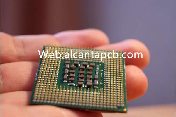
GPU (그래픽 처리 장치) 패키지 기판은 현대 컴퓨팅의 필수 구성 요소입니다., GPU의 다양한 전자 부품을 장착하고 상호 연결하기 위한 기반 플랫폼을 제공합니다.. 이러한 기판은 고성능 그래픽 처리에 필요한 고밀도 통합 및 효율적인 열 관리를 지원하도록 설계되었습니다.. GPU가 다양한 애플리케이션에서 점점 더 중요해짐에 따라, 게임 및 전문 그래픽부터 인공 지능 및 과학 컴퓨팅까지, GPU 패키지 기판의 역할이 그 어느 때보다 중요해졌습니다.. 이 기사에서는 속성을 살펴봅니다., 구조, 재료, 제조 공정, 애플리케이션, GPU 패키지 기판의 장점.
GPU 패키지 기판이란 무엇입니까??
GPU 패키지 기판은 그래픽 처리 장치의 구성 요소를 조립하고 상호 연결하는 데 사용되는 기본 재료 유형입니다.. 실리콘 칩과 인쇄회로기판 사이의 중개자 역할을 합니다. (PCB), 기계적 지원 및 전기적 연결 제공. GPU 패키지 기판은 최신 GPU에 필요한 고밀도 배선 및 복잡한 상호 연결을 수용하도록 설계되었습니다..
GPU 패키지 기판은 일반적으로 뛰어난 전기 절연성을 제공하는 고급 소재로 만들어집니다., 열전도도, 기계적 안정성. GPU 패키징에 필수적입니다., 섬세한 반도체 부품을 보호하고 고성능 조건에서 효율적으로 작동할 수 있도록 보장.
GPU 패키지 기판의 구조
GPU 패키지 기판의 구조는 복잡하고 다층적입니다., 고성능 그래픽 처리의 까다로운 요구 사항을 충족하도록 설계되었습니다.. 주요 구조 요소는 다음과 같습니다:
코어층은 기판의 기본 구조를 형성합니다., 기계적 안정성과 강성을 제공. 일반적으로 유리 섬유 강화 에폭시 수지 또는 세라믹과 같은 재료로 만들어집니다..
이 레이어는 코어 레이어 위에 추가되어 배선 밀도를 높이고 복잡한 회로 패턴을 지원합니다.. 최적의 전기적 성능을 보장하기 위해 고급 유전체 재료를 사용하여 빌드업 레이어를 구성했습니다..
전도성 층, 일반적으로 구리로 만들어짐, 기판의 다양한 구성 요소를 상호 연결하는 회로 트레이스를 형성합니다.. 이러한 레이어는 정밀하고 밀도가 높은 배선을 생성하기 위해 포토리소그래피 공정을 사용하여 패턴화됩니다..
비아는 기판의 서로 다른 레이어를 연결하는 수직 상호 연결입니다.. 고급 드릴링 기술을 사용하여 생성됩니다., 레이저 드릴링과 같은, 높은 정밀도와 신뢰성을 보장하기 위해.
표면 마감, 무전해 니켈 침지 금과 같은 (동의하다) 또는 유기 납땜성 보존제 (OSP), 납땜성을 향상시키고 산화를 방지하기 위해 접촉 패드에 적용됩니다..
환경적 손상으로부터 전도성 트레이스를 보호하고 조립 중 솔더 브리지를 방지하기 위해 솔더 마스크가 적용됩니다..
GPU 패키지 기판에 사용되는 재료이자형에스
GPU 패키지 기판의 재료 선택은 성능과 신뢰성에 매우 중요합니다.. 주요 자료는 다음과 같습니다:
에폭시 수지, 종종 유리섬유로 강화됨, 코어 및 빌드업 레이어에 일반적으로 사용됩니다.. 이 소재는 우수한 기계적 강도와 열 안정성을 제공합니다..
고성능 세라믹, 알루미나, 질화알루미늄 등, 우수한 열 전도성과 전기 절연성을 제공하기 위해 일부 GPU 패키지 기판에 사용됩니다..
구리는 우수한 전기 전도성으로 인해 전도성 층으로 널리 사용됩니다.. 얇은 구리 포일을 기판에 적층하고 패턴화하여 회로 트레이스를 형성합니다..
유전 상수와 손실 탄젠트가 낮은 고급 유전체 재료를 사용하여 신호 감쇠를 최소화하고 고주파수 성능을 보장합니다..
ENIG 및 OSP는 납땜성을 개선하고 접촉 패드를 산화 및 부식으로부터 보호하기 위해 일반적으로 사용되는 표면 마감재입니다..
GPU 패키지 기판 제조 공정
GPU 패키지 기판의 제조 공정에는 고품질과 성능을 보장하기 위해 정밀하고 제어된 여러 단계가 포함됩니다.. 주요 단계는 다음과 같습니다:
고품질 원료, 에폭시 수지를 포함한, 구리 포일, 및 유전체 필름, 요구되는 사양을 충족하는지 확인하기 위해 준비되고 검사됩니다..
코어층과 빌드업층을 열과 압력을 이용해 적층하여 일체형 기판을 형성합니다.. 이 단계에는 레이어가 적절하게 접착되었는지 확인하기 위한 정밀한 정렬 및 제어가 포함됩니다..
비아와 스루홀을 기판에 뚫어 층 사이에 전기적 상호 연결을 생성합니다.. 그런 다음이 구멍은 구리로 도금되어 전도성 경로를 설정합니다..
회로 패턴은 포토리소그래피 공정을 사용하여 생성됩니다.. 여기에는 감광성 필름을 적용하는 작업이 포함됩니다. (포토 레지스트) 구리 표면에, 자외선에 노출시켜 (UV) 마스크를 통해 빛, 노출된 영역을 개발하여 원하는 회로 패턴을 나타냅니다.. 그런 다음 기판을 에칭하여 원하지 않는 구리를 제거합니다., 회로 흔적을 남기고.
솔더 마스크는 기판에 적용되어 회로를 보호하고 조립 중 솔더 브리지를 방지합니다.. 솔더 마스크는 일반적으로 스크린 인쇄 또는 사진 이미징 기술을 사용하여 적용한 다음 경화하여 경화시킵니다..
접점 패드에 표면 마감 처리를 적용하여 납땜성을 강화하고 산화를 방지합니다.. 신뢰할 수 있는 솔더 조인트와 장기적인 내구성을 보장하기 위해 ENIG 또는 OSP와 같은 기술이 사용됩니다..
최종 기판은 모든 성능 및 신뢰성 표준을 충족하는지 확인하기 위해 엄격한 검사와 테스트를 거칩니다.. 전기 테스트, 육안 검사, 자동화된 광학 검사 (AOI) 결함이나 불규칙성을 식별하는 데 사용됩니다..
GPU 패키지 기판의 응용 분야
GPU 패키지 기판은 다양한 산업 분야의 광범위한 전자 응용 분야에 사용됩니다.. 주요 응용 분야는 다음과 같습니다.:
GPU는 게임 콘솔에서 고해상도 그래픽을 렌더링하는 데 필수적입니다., PC, 및 가상 현실 시스템. GPU 패키지 기판은 이러한 까다로운 애플리케이션에 필요한 성능과 안정성을 제공합니다..
애니메이션 등의 산업에서, 영화 제작, 그리고 그래픽 디자인, GPU는 복잡한 그래픽과 시각 효과를 렌더링하는 데 사용됩니다.. GPU 패키지 기판은 이러한 전문 애플리케이션의 고성능 요구 사항을 지원합니다..
GPU는 병렬 처리 기능으로 인해 AI 및 기계 학습 작업에 점점 더 많이 사용되고 있습니다.. GPU 패키지 기판은 AI 워크로드에 필요한 고밀도 통합 및 효율적인 열 관리를 가능하게 합니다..
과학 연구 및 시뮬레이션에서, GPU는 복잡한 계산과 데이터 분석을 가속화합니다.. GPU 패키지 기판은 이러한 고위험 애플리케이션에서 안정적인 성능을 보장합니다..
GPU는 고급 운전자 지원 시스템에 사용됩니다. (ADAS) 그리고 자율주행 기술. GPU 패키지 기판은 이러한 자동차 애플리케이션에 필요한 성능과 내구성을 제공합니다..
GPU 패키지 기판의 장점
GPU 패키지 기판은 최신 컴퓨팅 애플리케이션에 없어서는 안 될 여러 가지 장점을 제공합니다.. 이러한 장점은 다음과 같습니다:
GPU 패키지 기판은 전자 부품의 고밀도 통합을 지원합니다., 복잡한 기능의 통합을 가능하게 하고 전반적인 성능을 향상시킵니다..
GPU 패키지 기판에 사용된 고급 소재와 정밀한 제조 공정으로 신호 손실과 간섭을 최소화합니다., 결과적으로 우수한 전기적 성능을 발휘합니다..
GPU 패키지 기판은 열을 효과적으로 방출하도록 설계되었습니다., 과열을 방지하고 GPU 구성 요소의 안정적인 작동을 보장합니다..
GPU 패키지 기판에 사용된 견고한 구조와 고품질 소재는 까다로운 환경에서도 안정적인 성능을 보장합니다.. 이러한 기판은 열 순환을 견디도록 설계되었습니다., 기계적 응력, 그리고 가혹한 조건.
FAQ
GPU 패키지 기판이 고성능 컴퓨팅 애플리케이션에 적합한 이유?
GPU 패키지 기판은 고밀도 통합으로 인해 고성능 컴퓨팅 애플리케이션에 적합합니다., 향상된 전기적 성능, 효율적인 열 관리, 견고한 기계적 특성. 이러한 특성을 통해 까다로운 환경에서도 안정적이고 효율적인 작동이 가능합니다..
GPU 패키지 기판을 고온 환경에서 사용할 수 있습니까??
예, GPU 패키지 기판은 고온 환경에 매우 적합합니다.. 뛰어난 열 관리 기능과 견고한 구조로 열 스트레스 하에서도 안정적인 성능을 보장합니다., 게임 및 전문 그래픽과 같은 응용 프로그램에 이상적입니다..
GPU 패키지 기판은 어떻게 효과적인 열 관리를 보장합니까??
GPU 패키지 기판은 높은 열 전도성과 최적화된 열 설계를 갖춘 고급 소재를 사용하여 효과적인 열 관리를 보장합니다.. 이러한 기능은 GPU 구성 요소에서 기판으로의 효율적인 열 방출을 촉진합니다., 과열을 방지하고 안정적인 작동을 보장합니다..
GPU 패키지 기판을 사용하여 가장 큰 이점을 얻는 산업은 무엇입니까??
GPU 패키지 기판 사용으로 가장 큰 혜택을 받는 산업에는 게임과 엔터테인먼트가 포함됩니다., 전문 그래픽, 인공 지능, 과학 컴퓨팅, 그리고 자동차. 이러한 산업에는 고밀도 통합이 필요합니다., 향상된 전기적 성능, 효율적인 열 관리, 어떤 GPU 패키지 기판이 제공하는지.