CO., LTD")
Fabricant de circuits imprimés à grande vitesse. Un circuit imprimé à grande vitesse (PCB) le fabricant est spécialisé dans la production de PCB conçus pour gérer les signaux haute fréquence avec une dégradation minimale du signal. Ces fabricants utilisent des matériaux avancés et des techniques de fabrication précises pour garantir l'intégrité du signal., réduire les interférences électromagnétiques, et améliorer les performances. Leur expertise comprend la fabrication de PCB à impédance contrôlée, conceptions de traces optimisées, et stratifiés à grande vitesse. Idéal pour les applications en télécommunications, aérospatial, et calcul haute performance, ces fabricants proposent des solutions fiables et efficaces pour les systèmes électroniques exigeants.
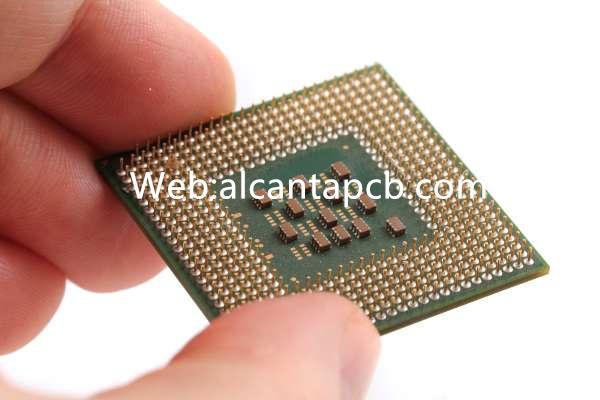
Cartes de circuits imprimés haute vitesse (PCBS) font partie intégrante des appareils électroniques modernes, en particulier ceux nécessitant une transmission et un traitement rapides des données. Ces PCBS sont spécialement conçus pour gérer les signaux haute fréquence, garantissant une perte de signal et des interférences minimales. Dans un monde où la vitesse est primordiale, que ce soit dans les télécommunications, calcul, ou traitement de données : les PCB à grande vitesse permettent le fonctionnement fiable de systèmes complexes. Cet article approfondit les caractéristiques, matériels, principes de conception, processus de fabrication, et applications des PCB haute vitesse, soulignant leur importance dans le paysage technologique actuel.
Qu'est-ce qu'un circuit imprimé haute vitesse?
Un circuit imprimé haute vitesse (PCB) est conçu pour gérer les signaux qui fonctionnent à hautes fréquences, souvent au-dessus 1 Ghz. Ces PCB sont essentiels pour les appareils où un transfert rapide de données est essentiel, comme dans les réseaux de communication, systèmes informatiques, et électronique avancée. La conception des PCB haute vitesse se concentre sur la préservation de l'intégrité du signal, réduire les interférences électromagnétiques (EMI), et minimiser l'atténuation du signal à tous les niveaux.
Dans les circuits à grande vitesse, le comportement des signaux électriques devient de plus en plus complexe, avec des facteurs comme la diaphonie, réflexion, et les déséquilibres d'impédance deviennent de plus en plus importants. Un PCB haute vitesse doit résoudre ces problèmes grâce à une conception et une sélection méticuleuses des matériaux., garantir que les signaux sont transmis avec un minimum de distorsion et de perte.
La construction de grande vitesse Les PCB impliquent souvent plusieurs couches, y compris les avions au sol et propulseurs, pour prendre en charge un routage complexe et maintenir l'intégrité du signal. La disposition du PCB doit tenir compte de la longueur et de l'impédance des traces, le placement des composants, et le potentiel de couplage électromagnétique entre traces adjacentes.
Les PCB haute vitesse sont essentiels dans des applications telles que la communication 5G, calcul haute performance, systèmes automobiles avancés, et l'électronique grand public, où le besoin d’une transmission de données rapide et fiable est primordial.
Matériaux utilisés dans les PCB haute vitesse
Les matériaux utilisés dans les PCB haute vitesse sont sélectionnés pour garantir des performances électriques optimales, gestion thermique, et stabilité mécanique. Ces matériaux doivent fournir une faible constante diélectrique (Dk), tangente à faible perte (Df), et d'excellentes propriétés thermiques. Les matériaux courants utilisés dans les PCB à grande vitesse comprennent:
Ces stratifiés, comme Rogers, Île, et Taconique, sont conçus pour les applications à grande vitesse. Ils offrent de faibles Dk et Df, qui aident à maintenir l’intégrité du signal à hautes fréquences. Ces matériaux ont également des propriétés électriques stables sur une large gamme de fréquences et de températures..
La qualité et l'épaisseur du cuivre utilisé dans les PCB haute vitesse sont essentielles pour garantir une transmission efficace du signal.. Des couches de cuivre plus épaisses sont souvent utilisées pour réduire les pertes résistives et prendre en charge des capacités de transport de courant plus élevées., tandis que les surfaces en cuivre ultra-lisses sont préférées pour minimiser l'atténuation du signal.
Préampe, un tissu en fibre de verre imprégné de résine, est utilisé pour lier les couches du PCB ensemble. Pour les applications à grande vitesse, des préimprégnés à faibles pertes sont utilisés pour maintenir l'intégrité du signal et réduire les pertes diélectriques.
Une gestion thermique efficace est cruciale dans les PCB à grande vitesse, car les signaux haute fréquence peuvent générer une chaleur importante. Matériaux à haute conductivité thermique, tels que les PCB à noyau métallique ou les substrats thermiquement conducteurs, sont utilisés pour dissiper efficacement la chaleur et éviter la surchauffe.
Dans les conceptions à grande vitesse, le contrôle de l'impédance des traces est essentiel pour éviter la réflexion et la distorsion du signal. Les matériaux prenant en charge un contrôle précis de l'impédance sont sélectionnés pour garantir une transmission cohérente du signal à travers le PCB..
Le choix des matériaux est influencé par les exigences spécifiques de l'application, y compris la vitesse du signal, consommation d'énergie, conditions environnementales, et la complexité globale du circuit.
Principes de conception pour les PCB haute vitesse
La conception d'un PCB haute vitesse implique de relever plusieurs défis clés pour garantir des performances et une fiabilité optimales.. Les principes de conception suivants sont essentiels à la conception de PCB à grande vitesse:
Le maintien de l'intégrité du signal est primordial dans la conception de PCB à grande vitesse. Cela implique un routage minutieux des traces pour minimiser la perte de signal, diaphonie, et EMI. Signalisation différentielle, où des paires de traces transportent des signaux complémentaires, est souvent utilisé pour améliorer l’intégrité du signal. La longueur des traces doit être soigneusement contrôlée pour éviter les problèmes de biais et de synchronisation..
Les signaux à grande vitesse sont sensibles aux désadaptations d'impédance, ce qui peut entraîner une réflexion et une dégradation du signal. L'impédance contrôlée est obtenue en définissant précisément la largeur de la trace, espacement, et propriétés des matériaux diélectriques. Cela garantit que l'impédance des traces correspond aux exigences des interfaces à haut débit.
Une alimentation électrique stable et sans bruit est essentielle pour les circuits à grande vitesse. La conception du PCB doit inclure des réseaux de distribution d'énergie à faible inductance (PDN), condensateurs de découplage, et des plans de masse bien conçus pour minimiser les fluctuations de tension et le bruit de puissance.
Une stratégie de mise à la terre solide est cruciale pour réduire les interférences électromagnétiques et maintenir l'intégrité du signal. Les plans de masse sont utilisés pour fournir un chemin de retour à faible impédance pour les signaux, tandis que des techniques de mise à la terre appropriées, tels que les vias de couture et les coulées au sol, sont utilisés pour empêcher le couplage des signaux et réduire le bruit.
Les circuits à grande vitesse peuvent générer une chaleur importante, qui doivent être gérés efficacement pour éviter une dégradation ou des dommages aux performances. La conception du PCB doit intégrer des vias thermiques, dissipateurs de chaleur, et d'autres solutions de refroidissement pour dissiper la chaleur et maintenir des températures de fonctionnement stables.
L'empilement des couches dans un PCB haute vitesse doit être soigneusement planifié pour équilibrer l'intégrité du signal, intégrité de l'alimentation, et gestion thermique. Les empilements multicouches sont souvent utilisés pour séparer les signaux à grande vitesse, avions à moteur, et plans de masse, réduisant le potentiel d'interférence du signal et améliorant les performances globales.
La diaphonie se produit lorsqu'un signal dans une trace induit un signal indésirable dans une trace adjacente.. Pour minimiser la diaphonie, les conceptions de PCB à grande vitesse utilisent un espacement plus large entre les traces, techniques de blindage, et paires différentielles.
La conception réussie d'un PCB haute vitesse nécessite une compréhension approfondie de la théorie électromagnétique, transmission des signaux, et dynamique thermique. Des outils de simulation avancés sont souvent utilisés pendant le processus de conception pour prédire le comportement des signaux à grande vitesse et optimiser la configuration du PCB..
Processus de fabrication de PCB haute vitesse
La fabrication de PCB haute vitesse comporte plusieurs étapes, chacun nécessitant précision et attention aux détails pour garantir que le produit final répond aux normes de haute performance requises pour les applications à grande vitesse. Les étapes clés du processus de fabrication comprennent:
Le processus commence par la sélection et la préparation des stratifiés haute fréquence appropriés., feuilles de cuivre, et matériaux préimprégnés. Ces matériaux sont ensuite laminés ensemble sous chaleur et pression pour former l'empilement multicouche de PCB..
Les PCB à grande vitesse nécessitent souvent un perçage précis pour les microvias, vias aveugles, et trous traversants, qui connectent différentes couches du PCB. Le perçage laser est couramment utilisé pour créer des microvias, tandis que le forage mécanique est utilisé pour les vias plus grands.
Les modèles de circuits sont transférés sur le PCB par photolithographie. Une résine photosensible est appliquée sur la surface, exposé à la lumière UV à travers un masque, puis développé pour révéler les traces de cuivre. Le cuivre exposé est gravé, quitter le motif de circuit souhaité.
Les vias et les trous traversants sont plaqués de cuivre pour établir des connexions électriques entre les couches. Une finition de surface, comme ENIG ou OSP, est ensuite appliqué pour protéger le cuivre et assurer une bonne soudabilité.
Un masque de soudure est appliqué pour protéger la surface du PCB de l'oxydation, éviter les ponts de soudure, et réduire les risques de courts-circuits. Le masque de soudure assure également une isolation entre les traces rapprochées.
Les composants sont placés sur le PCB à l'aide de machines automatisées de sélection et de placement. Les composants sont ensuite soudés au PCB en utilisant des techniques de brasage par refusion ou de brasage à la vague., en fonction des exigences de conception.
Le PCB final est soumis à des tests rigoureux pour garantir qu'il répond aux spécifications requises.. Les tests électriques vérifient l'intégrité du signal et le contrôle de l'impédance, tandis que les tests thermiques évaluent la capacité du PCB à gérer la chaleur. Des inspections visuelles sont également effectuées pour vérifier tout défaut de fabrication.
Le processus de fabrication des PCB haute vitesse nécessite un équipement avancé et un contrôle précis de chaque étape pour produire des cartes répondant aux exigences strictes des applications haute fréquence..
Applications des PCB haute vitesse
Les PCB haute vitesse sont cruciaux dans un large éventail d'applications où la transmission et le traitement rapides des données sont essentiels. Certaines des applications clés incluent:
En télécommunications, Les PCB haute vitesse sont utilisés dans des appareils tels que les routeurs, commutateurs, et stations de base, où ils permettent la transmission rapide de données sur les réseaux de communication. Ces PCB sont essentiels pour prendre en charge les exigences de bande passante élevée et de faible latence des systèmes de communication modernes..
Les PCB haute vitesse sont utilisés dans les supercalculateurs, centres de données, et systèmes HPC pour faciliter le traitement et le stockage rapides des données. Ces PCB assurent le fonctionnement efficace des processeurs, modules de mémoire, et interfaces haut débit dans des environnements informatiques exigeants.
Les PCB haute vitesse se trouvent dans les smartphones, comprimés, et autres appareils électroniques grand public qui nécessitent un transfert et un traitement rapides des données. Ces PCB prennent en charge les performances des interfaces haute vitesse, comme USB 3.0, HDMI, et PCIe, dans des appareils compacts et économes en énergie.
Dans l'industrie automobile, Les PCB haute vitesse sont utilisés dans les systèmes avancés d'aide à la conduite (ADAS), systèmes d'infodivertissement, et technologies de conduite autonome. Ces PCB permettent le traitement rapide des données des capteurs et le fonctionnement fiable des systèmes critiques pour la sécurité..
Les PCB haute vitesse sont utilisés dans les équipements d'imagerie médicale, appareils de diagnostic, et systèmes de surveillance des patients. Ces PCB garantissent le traitement précis et rapide des données médicales, permettant un diagnostic et un traitement fiables.
Les PCB haute vitesse sont utilisés dans les applications aérospatiales et de défense, y compris les systèmes radar, équipement de communication, et avionique. Ces PCB doivent résister aux environnements difficiles tout en conservant des performances et une fiabilité élevées.
Avantages de la haute vitesse PCBS
Les PCB haute vitesse offrent plusieurs avantages qui les rendent indispensables dans les systèmes électroniques modernes. Ces avantages comprennent:
Les PCB haute vitesse sont conçus pour prendre en charge une transmission rapide des données, permettant le fonctionnement efficace des circuits haute fréquence et réduisant la latence dans les systèmes de communication.
Les PCB haute vitesse sont conçus pour minimiser la perte de signal, diaphonie, et EMI, assurer la transmission précise des signaux haute fréquence.
En optimisant la conception et les matériaux des PCB, Les PCB haute vitesse peuvent atteindre des performances élevées tout en minimisant la consommation d'énergie, ce qui est essentiel pour les appareils économes en énergie.
Les PCB haute vitesse permettent l'intégration de circuits complexes dans des conceptions compactes et légères, ce qui les rend idéaux pour les applications portables et à espace limité.
Les PCB haute vitesse sont conçus pour résister aux exigences de fonctionnement à haute fréquence et aux conditions environnementales difficiles, garantissant une fiabilité et une durabilité à long terme.
FAQ
Quelles sont les principales considérations lors de la conception de PCB haute vitesse?
Les considérations clés incluent l'intégrité du signal, impédance contrôlée, intégrité de l'alimentation, techniques de mise à la terre, gestion thermique, et minimiser la diaphonie.
Quels matériaux sont couramment utilisés dans les PCB haute vitesse?
Les matériaux courants incluent les stratifiés haute fréquence (comme Rogers et Isola), revêtement en cuivre, matériaux préimprégnés à faibles pertes, et substrats de gestion thermique.
Quelles applications utilisent les PCB haute vitesse?
Les applications incluent les télécommunications, calcul haute performance, électronique grand public, électronique automobile, dispositifs médicaux, et systèmes aérospatiaux et de défense.
Comment sont fabriqués les PCB haute vitesse?
Le processus de fabrication implique la préparation des matériaux, laminage, forage, modelage, gravure, placage, placement des composants, assemblée, et des tests rigoureux pour garantir des performances et une fiabilité élevées.