CO., LTD")
Fabricant de PCB IPC classe III. En tant que fabricant de PCB IPC classe III, nous sommes spécialisés dans la production de circuits imprimés de haute fiabilité répondant aux normes de qualité et de performance les plus strictes. Nos produits sont conçus pour des applications exigeantes dans l'aérospatiale, médical, et industries militaires, où la précision et la durabilité sont primordiales. Avec des processus de fabrication de pointe et un contrôle qualité rigoureux, nous veillons à ce que chaque PCB dépasse les références de l'industrie, offrant des performances exceptionnelles dans les environnements critiques.
Qu'est-ce que le PCB IPC CLASSE III?
Classe IPC III PCB fait référence à une carte de circuit imprimé qui répond aux exigences les plus élevées de l'International Electronics Industry Connection Association (CIB) standard. IPC est l'organisme qui définit les normes mondiales d'interconnexion électronique, et ses normes sont largement utilisées dans l'industrie de la fabrication électronique. La conception, le processus de fabrication et de test des PCB IPC Classe III doit suivre des spécifications extrêmement strictes pour garantir leur stabilité et leur longue durée de vie dans des environnements difficiles.
Les PCB IPC Classe III sont principalement utilisés dans les domaines qui nécessitent une fiabilité extrêmement élevée et des exigences de performances strictes., comme l'aérospatiale, matériel militaire et médical. Ces scénarios d'application ont généralement des exigences extrêmement élevées en matière de fiabilité., durabilité et performances des équipements électroniques, et tout échec ou défaillance peut entraîner de graves conséquences. Par exemple, dans le domaine aérospatial, Les PCB dans les systèmes de contrôle doivent maintenir un fonctionnement stable à des températures extrêmes, environnements de pressions et de vibrations. Dans les applications militaires, Les PCB des systèmes de radar et de communication doivent pouvoir résister aux environnements difficiles des champs de bataille.. Dans le matériel médical, Les PCB présents dans les systèmes de survie et les instruments de diagnostic avancés doivent fonctionner sans problème pour garantir la sécurité des patients..
Afin de répondre à ces exigences strictes, Classe IPC III PCBS doit prendre en compte plusieurs facteurs clés lors de la phase de conception. Le premier est la sélection des matériaux. Des matériaux de substrat de haute qualité sont généralement utilisés, comme FR-4, polyimide (Polyimide) et substrats céramiques, etc.. pour assurer ses performances et sa stabilité dans des conditions de température et de pression élevées. Vient ensuite la conception des circuits, ce qui nécessite un calcul et une disposition précis pour réduire les interférences et les pertes de signal et garantir des performances électriques stables.
Pendant le processus de fabrication, Le PCB IPC Classe III utilise une technologie et des processus de fabrication avancés. Y compris l'empilement multicouche, gravure de précision, interconnexion haute densité (HDI) et d'autres technologies pour réaliser une intégration haute densité de circuits complexes. La précision requise pour le perçage et les connexions inter-couches est très élevée pour assurer des connexions fiables entre les couches. En outre, technologie de montage en surface (Smt) et technologie traversante (THT) sont largement utilisés dans le montage de composants pour améliorer l'efficacité et la fiabilité de l'assemblage.
Le lien de test est également une étape cruciale dans le processus de fabrication des PCB IPC Classe III.. Chaque PCB doit subir des tests stricts de performances électriques et des tests de performances mécaniques pour garantir qu'il répond aux normes IPC Classe III.. Ces tests incluent des tests de continuité électrique, test de résistance d'isolement, tests de cycle thermique et tests de vibrations pour simuler diverses situations possibles dans l'environnement d'utilisation réel et garantir la fiabilité et la durabilité du PCB.
En résumé, Le PCB IPC Classe III est une carte de circuit imprimé conçue et fabriquée spécifiquement pour des exigences élevées de fiabilité et de performance.. Ses spécifications strictes en matière de conception, sélection des matériaux, le processus de fabrication et les tests garantissent ses excellentes performances dans les applications critiques telles que l'aérospatiale, militaire et médical. En utilisant des PCB IPC Classe III, les ingénieurs et les fabricants peuvent garantir que leurs produits électroniques peuvent fonctionner de manière stable et fiable dans les environnements les plus exigeants.
Guide de référence de conception de circuits imprimés IPC CLASSE III.
La conception d'un PCB IPC Classe III nécessite la prise en compte de nombreuses normes et spécifications spécifiques pour garantir sa stabilité et ses hautes performances dans des environnements difficiles.. Cet article présentera en détail les règles de conception, directives de conception de configuration et de gestion thermique qui doivent être suivies lors de la conception de PCB IPC classe III.
Lors de la conception d'un PCB IPC Classe III, vous devez respecter strictement les normes IPC-2221 et IPC-2222, qui fournissent des conseils complets pour la conception de circuits imprimés afin de garantir les performances électriques et la stabilité mécanique. La norme IPC-2221 couvre les exigences de conception courantes, y compris les paramètres de base tels que la largeur du conducteur, espacement, ouvertures et nombre de couches. La norme IPC-2222 se concentre davantage sur les détails de conception de types spécifiques de PCB, comme unilatéral, panneaux double face et multicouches.
Spécifiquement, IPC-2221 et IPC-2222 exigent que les concepteurs prennent en compte la capacité actuelle, intégrité du signal, et gestion thermique lors de la sélection des matériaux et de la détermination de la largeur et de l'espacement des chemins conducteurs. Pour PCB IPC classe III, les règles de conception sont plus strictes en raison de son application dans des domaines à haute fiabilité tels que l'aérospatiale et les équipements médicaux. Par exemple, les largeurs et l'espacement des conducteurs doivent être plus larges et plus grands que les PCB classiques pour réduire le risque de panne électrique, tandis que des tests électriques complets sont nécessaires pour garantir qu'il n'y a pas de courts-circuits ou d'ouvertures.
La conception du schéma est un maillon clé dans la conception de circuits imprimés IPC Classe III. Cela nécessite un calcul précis de la disposition et du routage des composants pour réduire les interférences et la perte de signal.. Dans les applications haute fréquence, l'intégrité du signal est essentielle, des mesures doivent donc être prises pour éviter les réflexions du signal et les interférences électromagnétiques (EMI).
D'abord, la disposition des composants doit être aussi compacte que possible pour raccourcir le chemin du signal, réduisant ainsi l'impact de l'inductance et de la résistance sur le signal. En même temps, les composants sensibles au bruit doivent être tenus à l'écart des composants haute puissance ou haute fréquence pour éviter les interférences mutuelles. La conception de l’alimentation électrique et des fils de terre est également cruciale. La conception de cartes multicouches est généralement adoptée, et les couches d'alimentation et de masse sont placées respectivement sur la couche intermédiaire pour réduire le bruit de l'alimentation et l'effet de rebond au sol..
En outre, dans la conception du câblage, l'adaptation d'impédance caractéristique du signal doit être prise en compte, en particulier dans la transmission de signaux à grande vitesse. Des impédances incompatibles peuvent provoquer des réflexions et des distorsions du signal, affectant la stabilité du système. Grâce à un câblage approprié et à l'utilisation de paires différentielles, l'impédance peut être contrôlée efficacement pour garantir l'intégrité du signal.
La gestion thermique est un aspect important qui ne peut être ignoré lors de la conception de PCB IPC Classe III. Étant donné que les équipements hautes performances fonctionnent souvent dans des environnements à haute puissance et à haute température, des mesures efficaces de dissipation de la chaleur doivent être prises pour éviter la dégradation des performances et les pannes causées par une surchauffe.
D'abord, l'effet de dissipation thermique peut être amélioré en sélectionnant des matériaux de substrat à haute conductivité thermique, tels que des substrats céramiques ou des matériaux composites contenant des charges thermoconductrices. Deuxièmement, la disposition raisonnable des composants et la conception du câblage aident également à répartir la chaleur uniformément et à éviter la formation de points chauds.
En outre, les concepteurs devraient envisager d'ajouter des vias de dissipation thermique (via) pour conduire la chaleur des zones à haute température vers les zones à basse température, ou directement au dissipateur thermique. Pour les composants haute puissance, tels que des amplificateurs de puissance ou des circuits intégrés de gestion de l'alimentation, des zones spéciales de dissipation thermique peuvent être conçues sur le PCB, et des dissipateurs de chaleur ou des ventilateurs peuvent être installés si nécessaire pour améliorer encore l'effet de dissipation thermique.
La conception de PCB IPC Classe III nécessite le strict respect des normes IPC-2221 et IPC-2222 pour garantir qu'il répond aux exigences les plus élevées en termes de performances électriques et de stabilité mécanique.. Grâce à une conception d'aménagement précise et à des mesures de gestion thermique efficaces, les concepteurs peuvent atteindre des performances élevées, PCB de haute fiabilité qui répondent aux besoins d'applications exigeantes telles que l'aérospatiale, matériel militaire et médical. Ces directives de conception garantissent non seulement la stabilité et la fiabilité du PCB, mais aussi poser une base solide pour réaliser des produits électroniques complexes et sophistiqués.
Quel matériau est utilisé dans le PCB IPC CLASSE III?
Les PCB IPC Classe III comportent généralement des matériaux de haute qualité pour répondre à leurs exigences de performances dans des environnements extrêmes.. Voici quelques matériaux couramment utilisés:
FR-4 (Époxy renforcé de fibre de verre): Le FR-4 est l'un des matériaux de substrat PCB les plus courants et offre une excellente résistance mécanique et une excellente isolation électrique.. Il peut résister à des environnements à haute température et à forte humidité et fournir des performances stables. Dans PCB classe III IPC, l'utilisation du FR-4 garantit la fiabilité et la durabilité de la carte.
Polyimide: Le polyimide est un plastique technique haute performance avec une excellente résistance à la chaleur et une excellente stabilité chimique. Les PCB IPC Classe III sont couramment utilisés dans les applications qui nécessitent des températures élevées et des opérations à haute fréquence., telles que les applications aérospatiales et militaires.
Substrats céramiques: Les substrats céramiques constituent un choix idéal pour les applications nécessitant une conductivité thermique et une isolation électrique extrêmement élevées.. Ils peuvent dissiper efficacement la chaleur et maintenir des performances électriques stables, ils sont donc souvent utilisés dans des conceptions de circuits spéciaux haute puissance et haute fréquence dans les PCB IPC classe III.
Substrat métallique: Le substrat métallique présente de bonnes propriétés de dissipation thermique et est souvent utilisé dans des applications nécessitant une densité de puissance élevée et des performances stables.. Dans PCB classe III IPC, le substrat en aluminium et le substrat en cuivre sont des choix courants, particulièrement adapté aux domaines tels que l'éclairage LED et les équipements électroniques de puissance.
Les matériaux ci-dessus ont subi un contrôle de qualité et des tests stricts pour garantir qu'ils répondent aux normes et exigences des PCB IPC Classe III.. Le choix des bons matériaux est crucial pour garantir la stabilité et la fiabilité des PCB dans des environnements extrêmes, et ces matériaux peuvent répondre aux exigences de haute performance des PCB IPC Classe III.
Quelle est la taille du PCB IPC CLASSE III?
Dans la conception et la fabrication de produits électroniques hautes performances, Les PCB IPC Classe III sont privilégiés pour leur fiabilité supérieure et leurs normes de qualité strictes. Ce type de PCB est largement utilisé dans des domaines tels que l'aérospatiale, équipements militaires et médicaux qui nécessitent des performances et une fiabilité extrêmement élevées. Cet article détaillera les dimensions des PCB IPC Classe III ainsi que leur importance et leur impact dans différentes applications..
Les PCB IPC Classe III sont disponibles dans une large gamme de tailles en fonction de leur application et des exigences de conception.. Voici quelques tailles et scénarios d'application courants:
Les petits PCB IPC de classe III sont particulièrement courants dans les appareils électroniques grand public et les appareils portables.. Par exemple, smartphones, comprimés, et les appareils portables nécessitent tous des circuits imprimés de petite taille et dotés de fonctionnalités puissantes.. Ce type de PCB est généralement de petite taille, allant de quelques centimètres carrés à des dizaines de centimètres carrés. Malgré leur petite taille, ces PCB sont toujours capables de fournir une fiabilité élevée et d'excellentes performances grâce à l'utilisation de matériaux de haute qualité et de processus de fabrication de précision.
Les PCB IPC Classe III de taille moyenne sont largement utilisés dans les équipements médicaux, systèmes de contrôle industriels, et électronique automobile. La taille de ce type de PCB varie généralement de quelques dizaines à plusieurs centaines de centimètres carrés.. Les PCB de taille moyenne doivent intégrer davantage de modules fonctionnels dans un espace relativement compact tout en garantissant les performances électriques et l'intégrité du signal.. Par exemple, cartes de circuits imprimés de commande dans les équipements d'imagerie médicale et cartes de circuits imprimés dans les unités de commande automobiles (COUVERTURE) tomber dans cette catégorie.
Les grands PCB IPC de classe III sont principalement utilisés dans des applications telles que les équipements aérospatiaux et militaires qui nécessitent le traitement de signaux complexes et une puissance élevée.. La taille de ce type de PCB peut atteindre des centaines de centimètres carrés ou plus, et est souvent utilisé dans des domaines critiques tels que les satellites, systèmes radar et systèmes de contrôle d'aéronefs. Les grands PCB doivent gérer des conceptions de circuits complexes et des structures multicouches pour prendre en charge la transmission de signaux haute fréquence et des exigences de puissance élevées tout en conservant une fiabilité et une durabilité extrêmement élevées..
Lors de la conception de PCB IPC classe III, la taille n'est pas seulement un paramètre physique, cela affecte également directement les performances électriques, gestion thermique, et les coûts de fabrication. Voici quelques considérations de conception:
Les PCB plus gros peuvent nécessiter des fils plus longs, ce qui peut provoquer des retards de signal et des interférences. Les concepteurs doivent planifier soigneusement la conception de la configuration pour garantir l'intégrité du signal..
À mesure que la taille du PCB augmente, les problèmes de dissipation thermique deviennent plus complexes. Les concepteurs doivent envisager l'utilisation de dissipateurs thermiques, matériaux thermoconducteurs et ventilation adéquate pour garantir une dissipation efficace de la chaleur.
Des tailles de PCB plus grandes signifient généralement des coûts de matériaux et de fabrication plus élevés. Les concepteurs doivent trouver un équilibre entre performances et coûts pour garantir que le produit final répond aux exigences de performances tout en étant rentable..
Les tailles de PCB IPC classe III varient selon l'application, des petits appareils portables aux grands systèmes aérospatiaux, tous avec des exigences de taille spécifiques. Quelle que soit la taille, ces PCB doivent répondre à des normes strictes de performance et de fiabilité. Grâce à une conception raisonnable et à des processus de fabrication précis, Les PCB IPC Classe III peuvent fournir d'excellentes performances et fiabilité dans diverses conditions extrêmes, assurer un fonctionnement stable des applications critiques. Comprendre les caractéristiques et les considérations de conception des PCB de différentes tailles peut aider les ingénieurs et les concepteurs à mieux développer des produits électroniques hautes performances répondant à divers besoins..
Le processus de fabrication des PCB IPC CLASSE III.
Le processus de fabrication des PCB IPC Classe III est complexe et précis, exigeant le strict respect de diverses normes et spécifications pour garantir ses performances dans des applications hautes performances et haute fiabilité. Vous trouverez ci-dessous les étapes détaillées de la fabrication de PCB IPC classe III:
D'abord, la sélection du matériau de substrat approprié est une étape critique dans la fabrication d'un PCB IPC classe III de haute qualité. Les matériaux de substrat couramment utilisés incluent le FR-4, substrats en polyimide et en céramique. Les matériaux doivent être sélectionnés en tenant compte de leurs propriétés électriques, résistance mécanique et résistance thermique. Une fois le matériau du substrat sélectionné, il doit être prétraité pour garantir que sa surface est propre et adaptée aux étapes de traitement ultérieures. Cela comprend le nettoyage, séchage et rugosité de la surface pour améliorer l'adhérence de la feuille de cuivre.
La formation de modèles de feuilles de cuivre est l'une des étapes essentielles de la fabrication des PCB.. D'abord, une couche de feuille de cuivre est recouverte sur le substrat, puis le motif de circuit requis est transféré sur la feuille de cuivre grâce à la technologie de photolithographie. Suivant, une gravure chimique est utilisée pour éliminer la feuille de cuivre non protégée, ne laissant que les chemins conducteurs conçus. Pour circuits de précision et haute densité, technologie d'écriture directe laser plus avancée (ILD) peut être utilisé pour garantir une plus grande précision et cohérence.
La fabrication de PCB multicouches nécessite la stratification de plusieurs couches les unes sur les autres.. Chaque couche est constituée de motifs individuels en feuille de cuivre séparés par un matériau isolant tel qu'un préimprégné.. Pendant le processus de laminage, une température et une pression élevées sont utilisées pour combiner étroitement les couches en un tout. Une fois le laminage terminé, un perçage est nécessaire pour réaliser les connexions électriques entre les couches. Le perçage peut être effectué soit par perçage mécanique, soit par perçage laser., ce dernier étant adapté aux conceptions à haute densité et à petites ouvertures.
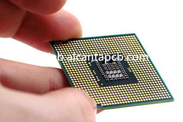
L'assemblage de composants est le processus de montage de composants électroniques sur un PCB. Les méthodes couramment utilisées sont la technologie de montage en surface (Smt) et technologie traversante (THT). SMT convient aux petits, composants légers et haute densité, souder des composants directement à la surface du PCB. THT, d'autre part, insère et soude les broches du composant au PCB à travers des trous pré-percés, ce qui convient aux composants plus grands et aux situations nécessitant des connexions mécaniques plus solides. Pendant le montage, un équipement automatisé est nécessaire pour un positionnement et un soudage précis afin de garantir la qualité et la cohérence.
Les tests de qualité sont une étape essentielle pour garantir que les PCB IPC Classe III répondent à des normes strictes.. Après avoir terminé l'assemblage, le PCB doit subir une série de tests électriques et mécaniques rigoureux. Les tests électriques comprennent les tests de circuits ouverts et de courts-circuits, tests fonctionnels, et tests haute tension pour garantir l'intégrité et les performances du circuit. Les tests mécaniques incluent les tests de cycle thermique, tests de vibrations et tests de chocs pour évaluer la fiabilité et la durabilité des PCB dans des conditions extrêmes. En outre, une inspection visuelle est nécessaire pour détecter d'éventuels défauts tels que de mauvais joints de soudure ou des défauts de câblage. Tous les résultats des tests doivent être enregistrés et examinés selon des procédures de contrôle de qualité strictes pour garantir que chaque PCB répond aux normes élevées de la classe IPC III..
Le processus de fabrication des PCB IPC Classe III nécessite non seulement un travail de haute précision et de haute qualité., mais aussi des procédures strictes de contrôle de qualité et de test. Grâce à une préparation minutieuse du support, motif précis de feuille de cuivre, stratification et perçage serrés, assemblage de composants fiable, et des tests de qualité complets, Les PCB IPC Classe III sont capables de fournir des performances et une fiabilité supérieures dans une variété d'applications exigeantes.. Applications dans l'aérospatiale, militaire, et les équipements médicaux ont prouvé leurs performances supérieures dans les conditions les plus exigeantes.
Le domaine d'application du PCB IPC CLASSE III.
Les PCB IPC Classe III jouent un rôle essentiel dans l'aérospatiale, domaines des équipements militaires et médicaux. Sa gamme d'applications couvre de nombreux scénarios qui nécessitent une fiabilité et des performances extrêmement élevées..
Dans le champ aérospatial, Le PCB IPC Classe III est largement utilisé dans les systèmes de contrôle des avions et des satellites. Ces systèmes effectuent des tâches clés telles que la navigation, communication, traitement des données et contrôle de vol, exigeant que les PCB fonctionnent de manière stable pendant une longue période dans des environnements spatiaux extrêmes. Les PCB IPC Classe III garantissent la sécurité et les performances des engins spatiaux grâce à des normes strictes de conception et de fabrication pour garantir leur fiabilité et leur durabilité dans des conditions telles qu'un rayonnement élevé., températures extrêmes et vide.
Dans le domaine militaire, Le PCB IPC Classe III est largement utilisé dans les équipements électroniques militaires, comme le radar, systèmes de communication, contrôle des missiles et drones, etc.. Ces équipements doivent souvent effectuer des missions de combat ou de reconnaissance dans des environnements extrêmement rudes., comme une température élevée, humidité élevée, haute altitude, et de fortes interférences électromagnétiques. La haute fiabilité et la durabilité des PCB IPC Classe III lui permettent de fonctionner de manière stable dans ces environnements difficiles., assurer la stabilité et l'efficacité au combat des systèmes militaires.
Dans le domaine du matériel médical, Les PCB IPC Classe III sont largement utilisés dans les équipements de survie et les instruments de diagnostic avancés.. Ces appareils ont des exigences extrêmement élevées en matière de fiabilité et de stabilité des composants électroniques, car ils sont directement liés à la sécurité et à la santé des patients.. Grâce à des normes de fabrication strictes et à un contrôle de qualité, Le PCB IPC Classe III garantit que l'équipement médical ne fonctionnera pas mal pendant un fonctionnement à long terme, garantissant ainsi l'exactitude et la fiabilité du diagnostic et du traitement médical.
En résumé, l'application des PCB IPC Classe III dans les domaines de l'aérospatiale, les équipements militaires et médicaux ne favorisent pas seulement le progrès technologique et l'innovation, mais fournit également un support technique fiable et une garantie pour le développement et le progrès de la société humaine.
Quels sont les avantages du PCB IPC CLASSE III?
Le principal avantage des PCB IPC Classe III est sa haute fiabilité supérieure à celle des autres types de PCB.. Cette haute fiabilité provient de normes strictes de fabrication et de test, garantissant que chaque PCB IPC Classe III peut fonctionner de manière stable pendant une longue période dans les applications critiques. Pendant le processus de fabrication, chaque étape est conforme aux normes IPC-6012 Classe III, qui couvrent des aspects tels que l’intégrité électrique, résistance mécanique et adéquation environnementale. Chaque étape du processus de production est strictement contrôlée et surveillée pour garantir que tous les PCB répondent aux exigences de qualité les plus élevées.. En outre, Les PCB IPC Classe III seront soumis à une série de tests rigoureux avant de quitter l'usine, y compris les tests électriques, essais de cycles thermiques et essais de vibrations mécaniques, pour vérifier leur fiabilité dans des conditions extrêmes.
Le PCB IPC Classe III excelle également en hautes performances. D'abord, son processus de conception utilise des outils de calcul et de simulation précis pour garantir que chaque chemin électrique et disposition des composants peut atteindre des performances optimales. La sélection de matériaux de haute qualité est également une garantie importante pour ses hautes performances. Généralement, ce type de PCB utilise des matériaux hautes performances tels que le FR-4, substrats en polyimide ou en céramique. Ces matériaux ont d'excellentes propriétés électriques et capacités de gestion thermique et peuvent maintenir des performances stables dans des environnements à haute fréquence et à haute température.. En outre, Le PCB IPC Classe III fonctionne également de manière exceptionnelle en termes d'intégrité du signal et de compatibilité électromagnétique. (EMC), ce qui peut réduire efficacement les interférences de signal et le bruit électromagnétique et assurer son fonctionnement normal dans des environnements électromagnétiques complexes.
La durabilité est un autre grand avantage des PCB IPC Classe III. Parce qu'ils sont conçus et fabriqués en vue d'une utilisation dans des conditions environnementales extrêmes., ce type de PCB a une longue durée de vie. Des matériaux de substrat de haute qualité et des processus de fabrication raffinés lui permettent de résister aux environnements difficiles tels que les températures élevées., basse température, humidité et corrosion chimique. En outre, Les PCB IPC Classe III ont également une excellente résistance mécanique et peuvent résister aux vibrations et aux chocs., ce qui est particulièrement important pour des applications telles que l'aérospatiale, matériel militaire et médical. Une durabilité accrue ne prolonge pas seulement la durée de vie de l'équipement, mais réduit également la fréquence de maintenance et de remplacement, réduire les coûts d’exploitation globaux.
Dans l'ensemble, la grande fiabilité, les performances et la durabilité des PCB IPC Classe III leur confèrent des avantages inégalés dans les applications critiques nécessitant une précision et une stabilité extrêmement élevées. Ces avantages en font le premier choix dans des domaines tels que l'aérospatiale, matériel militaire et médical haut de gamme. Bien que son coût de fabrication puisse être supérieur à celui d'un PCB ordinaire, ses excellentes performances et son faible taux de défaillance sur le long terme le rendent globalement plus rentable. Donc, Le PCB IPC Classe III n'est pas seulement un symbole de leadership technologique, mais aussi un gage de fiabilité et de performance, fournir une base solide pour diverses applications à forte demande.
Grâce à l'analyse détaillée ci-dessus, nous pouvons voir l'importance et les avantages des PCB IPC Classe III dans la technologie électronique moderne, fournir des solutions fiables et efficaces pour diverses applications à forte demande.
FAQ
Qu'est-ce qu'un PCB IPC classe III?
Les PCB IPC Classe III sont l'une des normes les plus élevées en matière de cartes de circuits imprimés et répondent aux exigences les plus élevées de l'IPC. (Association internationale pour la connectivité de l'industrie électronique) caractéristiques. Il est principalement utilisé dans les applications nécessitant une fiabilité et des performances extrêmement élevées., comme l'aérospatiale, matériel militaire et médical. Ce type de PCB doit suivre des normes strictes en matière de conception, fabrication et tests pour garantir sa stabilité et sa longue durée de vie dans des environnements difficiles.
En quoi les PCB IPC classe III sont-ils différents des autres classes de PCB?
Les PCB IPC Classe III ont une fiabilité plus élevée et des exigences de performance strictes que les autres classes de PCB, comme la classe I et la classe II. Il doit répondre à une conception plus stricte, normes de fabrication et de test pour s’adapter à des environnements d’application plus exigeants, comme des températures extrêmes, conditions de vibrations et d'humidité.
Comment choisir le matériau de substrat PCB approprié?
La sélection d'un matériau de substrat de PCB approprié nécessite la prise en compte de plusieurs facteurs, y compris l'environnement d'application, température de fonctionnement, résistance mécanique et performances électriques. Les matériaux de substrat courants incluent le FR-4, substrats en polyimide et en céramique. Chaque matériau a des caractéristiques différentes et convient à différents scénarios d'application.
Quels sont les facteurs qui affectent les coûts de fabrication des PCB?
Les facteurs qui affectent les coûts de fabrication des PCB incluent la sélection des matériaux, nombre de couches de PCB, complexité, taille du lot de production, et exigences en matière de tests. Typiquement, l'augmentation du nombre de couches et de la complexité augmente les coûts de fabrication, tandis que la production de masse réduit le coût par PCB.
Quelles sont les considérations environnementales pour la production et la manipulation des PCB?
Pendant le processus de production et de traitement des PCB, les facteurs environnementaux doivent être pris en compte, y compris la réduction de l’utilisation de substances nocives, gérer rationnellement les déchets et les eaux usées, et en respectant les réglementations environnementales en vigueur. Le choix de matériaux et de processus de fabrication respectueux de l'environnement est essentiel pour réduire l'impact environnemental.