CO., LTD")
PCB multicapa
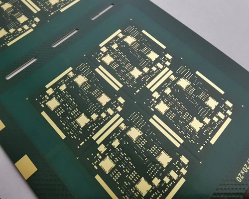
Fabricación de PCB, Ofrecemos PCB multicapa de 4 capa a 108 capa. PCB HDI. PCB HDI rígido-flexible. Híbridos & Dieléctricos mixtos, Tecnologías de vías enterradas y ciegas.
Los agujeros enterrados y los agujeros ciegos se definen de la siguiente manera
Vías ciegas: Una vía ciega es un tipo de vía que conecta la pista interna de la PCB con la pista de la superficie de la PCB.. Este agujero no penetra todo el tablero..
Vías enterradas: Las vías enterradas solo están conectadas al tipo de vías entre las capas internas., para que no sean visibles desde la superficie de la PCB.
Ventajas de la placa de circuito impreso con orificio ciego enterrado
- Elimine una gran cantidad de diseños de orificios pasantes y aumente la densidad del cableado y la densidad del paquete.;
- Diversificar y complicar el diseño de la estructura de interconexión del tablero multicapa.;
- Se mejoró significativamente la confiabilidad de las placas multicapa y el rendimiento eléctrico de los productos electrónicos..
Se distinguen los siguientes tres puntos para los tableros de placas enterrados a ciegas
- A diferencia del agujero pasante, el orificio pasante se refiere a un orificio a través del cual se perfora cada capa, y el agujero ciego es un agujero pasante no perforado.
- Subdivisión de agujero ciego: agujero ciego, agujero enterrado (la capa exterior no es visible).
- Distinguirse del proceso de producción.: Se perforan agujeros ciegos antes de presionar., y se perforan agujeros pasantes después de presionar.
La tecnología de orificios enterrados ciegos se utiliza principalmente en PCB de gama relativamente alta, con alto contenido técnico y altos requisitos para los fabricantes de placas PCB. Nuestro correo electrónico: info@alcantapcb.com