주식회사")
무선주파 PCB 제조업체. 선도적인 무선통신업체로서 빈도 PCB 제조업체, 우리는 현대 통신 시스템의 까다로운 요구 사항을 충족하는 고품질 RF PCB 생산을 전문으로 합니다.. 당사의 고급 제조 공정은 탁월한 신호 무결성을 보장합니다., 낮은 손실, 높은 신뢰성. 5G 네트워크 여부, 위성 통신, 또는 군사 응용 프로그램, 당사의 RF PCB는 뛰어난 성능과 내구성을 제공합니다., 우리를 최첨단 기술 솔루션에 대한 선호하는 선택으로 만듭니다..
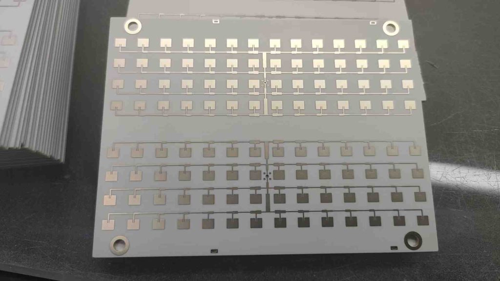
무선 주파수 (RF) PCB는 고주파수에서 작동하도록 설계된 특수 인쇄 회로 기판입니다.. 이 보드는 무선 주파수 신호를 정확하고 효율적으로 처리해야 하는 애플리케이션에 매우 중요합니다., 통신 분야와 같은, 무선 네트워크, 레이더 시스템, 및 기타 고주파 애플리케이션. RF PCB는 신호 손실을 최소화하기 위해 고유한 재료와 디자인으로 제작되었습니다., 높은 신호 무결성, 까다로운 환경에서도 안정적인 성능.
무선 주파수 PCB 란 무엇입니까??
RF PCB 고주파 신호를 처리하도록 특별히 설계된 인쇄 회로 기판의 일종입니다., 일반적으로 메가헤르츠 범위 (MHz) 기가헤르츠로 (GHz). 이 PCB는 전파의 전송 및 수신이 필수적인 장치 및 시스템에 사용됩니다.. RF PCB의 설계 및 구성에는 재료에 대한 세심한 주의가 필요합니다., 공들여 나열한 것, 원하는 전기적 성능과 신뢰성을 달성하기 위한 제조 공정.
RF PCB 설계에는 고주파수에서 최적의 성능을 보장하기 위한 몇 가지 중요한 고려 사항이 포함됩니다.. 다음 섹션에서는 RF PCB 설계의 주요 측면을 간략하게 설명합니다..
RF PCB에 사용되는 재료는 성능에 중요한 역할을 합니다.. 주요 자료에는 포함됩니다:
기판 재료: Rogers와 같은 고주파 기판, PTFE (테프론), 세라믹 충전 재료는 유전율이 낮기 때문에 일반적으로 사용됩니다. (DK) 낮은 소산 인자 (Df). 이러한 소재는 고주파수에서 신호 무결성을 유지하는 데 도움이 됩니다..
구리 포일: 전도성 트레이스 및 평면에 고순도 구리가 사용됩니다., 우수한 전기 전도성과 신뢰성 제공.
프리프레그 및 라미네이트: 고성능 프리프레그와 라미네이트 소재를 사용하여 레이어를 서로 접착합니다., 낮은 유전 손실과 높은 열 안정성 제공.
레이어 스택업은 RF PCB 설계의 중요한 측면입니다.:
신호층: 다중 신호 레이어는 고주파 신호를 라우팅하는 데 사용됩니다.. 이러한 레이어는 제어된 임피던스로 설계되어 신호 손실을 최소화하고 신호 무결성을 높입니다..
전원 및 접지면: 전용 전원 및 접지면은 안정적인 전압 레퍼런스를 제공하고 소음을 줄입니다., 이는 RF 애플리케이션에서 신호 무결성을 유지하는 데 중요합니다..
열 관리 계층: 고주파 부품에서 발생하는 열을 방출하기 위해 열 비아와 열 확산기가 통합되어 있습니다., 안정적인 성능 보장.
설계 단계에서 몇 가지 주요 고려 사항을 해결해야 합니다.:신호 무결성: 제어된 임피던스를 통해 높은 신호 무결성이 유지됩니다., 차동 쌍 라우팅, 기생 효과 최소화. 설계에서는 신호 경로가 최대한 짧고 직접적이어야 합니다..
배전: 전용 전력판을 통해 효율적인 전력 분배가 보장됩니다., 전압 강하를 최소화하고 RF 부품에 안정적인 전력 공급을 보장합니다..
열 관리: 효과적인 열 관리 기술, 열 비아 및 열 확산기 등, 과열을 방지하고 일관된 성능을 보장합니다..
기계적 안정성: 보드는 고주파 환경에서의 취급 및 작동 스트레스를 견딜 수 있도록 견고한 기계적 지지를 제공해야 합니다..
신뢰할 수 있음: 고품질 소재 사용과 정밀한 제조 공정을 통해 장기적인 신뢰성이 보장됩니다., 박리, 뒤틀림 등의 문제 방지.
RF PCB에 사용되는 재료?
RF PCB에 사용되는 재료는 전기적 특성을 위해 선택됩니다., 열의, 및 기계적 특성:
로저스 기판: Rogers 소재는 낮은 유전 상수와 낮은 손실로 인해 RF 애플리케이션에 널리 사용됩니다., 고주파수 성능에 필수적인.
PTFE (테프론): PTFE는 RF 기판에 널리 사용되는 또 다른 선택입니다., 우수한 전기적 특성과 낮은 유전 손실 제공.
세라믹 충전 재료: 이 재료는 높은 열 안정성과 낮은 유전 손실을 제공합니다., 고전력 RF 애플리케이션에 적합하게 만듭니다..
구리 포일: 전도성 트레이스 및 평면에 고순도 구리가 사용됩니다., 우수한 전기 전도성과 신뢰성 제공.
프리프레그 및 라미네이트: 고성능 프리프레그와 라미네이트 소재를 사용하여 레이어를 서로 접착합니다., 낮은 유전 손실과 높은 열 안정성 제공.
RF PCB의 크기는 얼마입니까??
RF PCB의 크기는 애플리케이션 및 특정 설계 요구 사항에 따라 다릅니다.:
두께: RF PCB의 두께는 다음과 같습니다. 0.5 mm ~ 수 밀리미터, 레이어 수와 열 관리 요구 사항에 따라 다름.
치수: PCB의 길이와 너비는 구성요소의 크기와 시스템의 레이아웃에 따라 결정됩니다.. 소형 장치용 소형 폼 팩터부터 복잡한 RF 시스템용 대형 보드까지 다양합니다..
RF PCB의 제조 공정
RF PCB의 제조 공정에는 높은 품질과 성능을 보장하기 위해 정밀하고 제어된 여러 단계가 포함됩니다.:
고성능 기판 소재, 구리 포일, 프리프레그 재료를 준비하고 가공에 적합한 크기로 절단합니다..
도전성 물질과 절연성 물질을 적층하여 적층하여 층을 형성함. 각 레이어는 회로를 정의하기 위해 포토리소그래피를 사용하여 패턴화됩니다..
마이크로비아 및 스루홀은 레이저 또는 기계적 드릴링 기술을 사용하여 드릴링됩니다.. 그런 다음 이 구멍을 구리로 도금하여 층 사이에 전기적 연결을 만듭니다..
개별 층은 열과 압력을 받아 함께 적층되어 고체를 형성합니다., 다층 구조. 이 과정을 통해 모든 레이어가 단단히 결합되고 정렬됩니다..
포토리소그래피 및 에칭 공정을 사용하여 각 레이어에 미세 피치 회로를 생성합니다., 정확한 상호 연결을 위해 높은 정밀도가 요구됨.
제작 후, 보드는 필요한 구성 요소와 커넥터로 조립됩니다.. 보드가 모든 설계 사양 및 성능 요구 사항을 충족하는지 확인하기 위해 엄격한 테스트가 수행됩니다..
RF PCB의 응용 분야
RF PCB는 광범위한 고주파 애플리케이션에 사용됩니다.:
통신에서, RF PCB는 기지국에 사용됩니다., 안테나, 안정적인 신호 전송 및 수신을 보장하는 기타 고주파 통신 장비.
항공우주 및 방위 산업 분야, RF PCB는 레이더 시스템에 사용됩니다., 통신 장비, 및 전자전 시스템, RF 신호의 정밀한 제어가 중요한 경우.
의료기기, RF PCB는 이미징 시스템에 사용됩니다., 진단 장비, 및 무선 통신 장치, 고주파 성능이 필수적인 곳.
테스트 및 측정 장비, RF PCB는 고주파 신호 테스트 및 분석을 지원하는 데 사용됩니다., 정확하고 신뢰할 수 있는 결과 보장.
RF PCB의 장점은 무엇입니까??
RF PCB는 고주파 애플리케이션에 없어서는 안 될 여러 가지 장점을 제공합니다.:
고성능: 우수한 전기적 특성을 제공합니다., 최소한의 손실로 안정적인 고주파 신호 전송 가능.
신호 무결성: 제어된 임피던스와 저손실 재료를 통해 높은 신호 무결성이 유지됩니다., 정확한 신호 전송 보장.
열 관리: 효과적인 열 관리 기술로 과열을 방지하고 고주파수에서 일관된 성능을 보장합니다..
기계적 안정성: 견고한 기계적 특성으로 인해 보드는 고주파 환경에서 취급 및 작동에 따른 스트레스를 견딜 수 있습니다..
신뢰할 수 있음: 고품질 소재와 정밀한 제조 공정으로 장기적인 신뢰성과 성능을 보장합니다..
FAQ
RF PCB 설계 시 주요 고려 사항은 무엇입니까??
주요 고려 사항에는 전기 및 열 성능을 위한 재료 선택이 포함됩니다., 복잡한 라우팅을 위한 레이어 스택업, 신호 무결성 보장, 전력 분배, 열 관리, 기계적 안정성, 신뢰성.
RF PCB는 표준 PCB와 어떻게 다른가요??
RF PCB는 고주파 애플리케이션용으로 특별히 설계되었습니다., 신호 손실을 최소화하기 위한 고급 소재와 디자인이 특징입니다., 표준 PCB는 성능 요구 사항이 덜 까다로운 일반 전자 응용 분야에 사용됩니다..
RF PCB의 일반적인 제조 공정은 무엇입니까??
이 과정에는 재료 준비가 포함됩니다., 레이어 제작, 드릴링 및 도금, 적층, 회로 패터닝, 집회, 높은 품질과 성능을 보장하기 위한 엄격한 테스트.
RF PCB의 주요 응용 분야는 무엇입니까??
이 PCB는 통신에 사용됩니다., 항공 우주 및 방어, 의료기기, 테스트 및 측정 장비, 고주파 애플리케이션에 고급 기능과 신뢰성 제공.