주식회사")
초박형 IC 패키지 기판 Manufacturer.우리는 초박형 IC 패키지 기판의 선두 제조업체입니다., 고성능 전자기기를 위한 최첨단 솔루션을 제공합니다.. 우리의 첨단 제조 기술은 탁월한 품질을 보장합니다., 다양한 응용 분야에서 소형화 및 기능 강화가 가능합니다., 스마트폰부터 의료기기까지. 혁신을 위해 우리를 믿으세요, 믿을 수 있는, 오늘날 기술 중심 세계의 요구 사항을 충족하는 효율적인 IC 패키지 기판.
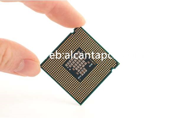
초박형 IC (집적 회로) 패키지 기판 현대 전자 제품의 필수 구성 요소입니다., 다양한 기기의 소형화 및 성능 향상을 가능하게 합니다.. 이 기판은 필요한 전기적 특성을 유지하면서 매우 얇게 설계되었습니다., 열의, 고성능 IC를 지원하는 기계적 특성. 초박형 기판은 공간이 부족한 응용 분야에서 특히 중요합니다., 스마트폰과 같은, 웨어러블 기기, 및 고급 컴퓨팅 시스템.
초박형 IC 패키지 기판이란??
초박형 IC 패키지 기판은 특수한 유형의 인쇄 회로 기판입니다. (PCB) IC를 장착하고 상호 연결하기 위한 플랫폼을 제공하도록 설계되었습니다.. 이 기판은 최소 두께가 특징입니다., 일반적으로 미만 100 마이크로미터, 초소형 전자 패키지 개발이 가능합니다.. 얇음에도 불구하고, 초박형 기판은 고밀도 상호 연결을 지원해야 합니다., 효율적인 열 관리, 호스팅하는 IC의 안정적인 작동을 보장하는 강력한 기계적 안정성.
초박형 IC 패키지 기판 설계 참조 가이드
초박형 IC 패키지 기판 설계에는 최적의 성능과 신뢰성을 보장하기 위한 포괄적인 접근 방식이 필요합니다..
초박형 기판에서 원하는 특성을 달성하려면 재료 선택이 중요합니다.:
고밀도 폴리이미드 필름: 이 소재는 뛰어난 유연성을 제공합니다., 높은 열 안정성, 그리고 전기 절연성이 좋아, 초박형 애플리케이션에 이상적입니다..
구리 포일: 전도성 트레이스 및 상호 연결에 사용됩니다., 구리 포일은 얇으면서도 내구성이 있어야 상당한 부피를 추가하지 않고도 전기적 성능을 유지할 수 있습니다..
접착제 및 유전체: 유전율이 낮고 열전도율이 높은 고급 접착제와 유전체 재료를 사용하여 층을 접착하고 절연성을 제공합니다..
초박형 기판의 레이어 구조는 공간 효율성과 성능을 극대화하도록 설계되었습니다.:
신호층: 이러한 레이어는 신호 손실과 누화를 최소화하도록 구성됩니다.. 제어된 임피던스를 유지하기 위해 마이크로스트립 및 스트립라인과 같은 기술이 사용됩니다..
전력 및 접지층: 안정적인 전력 분배와 소음 감소를 위해서는 전용 전원 및 접지면이 중요합니다., 안정적인 IC 작동 보장.
열 관리 계층: 열 비아와 열 확산기를 통합하면 열을 효과적으로 분산시키는 데 도움이 됩니다., 중요한 구성 요소의 과열 방지.
상호 연결 레이어: 고밀도 상호 연결 (HDI) 마이크로비아와 스루홀을 사용하면 초박형 기판의 제한된 공간 내에서 복잡한 라우팅이 가능합니다..
초박형 IC 패키지 기판에 사용되는 재료?
초박형 IC 패키지 기판에 사용되는 재료는 엄격한 성능 요구 사항을 충족할 수 있도록 선택되었습니다.:
고밀도 폴리이미드 필름: 뛰어난 유연성 제공, 열 안정성, 전기 절연, 이 필름은 초박형 응용 분야에 일반적으로 선택됩니다..
구리 포일: 얇지만 내구성이 뛰어난 구리 포일이 전도성 트레이스 및 상호 연결에 사용됩니다., 안정적인 전기적 성능 보장.
접착제 및 유전체: 유전율이 낮고 열전도율이 높은 고급 접착제와 유전체 재료를 사용하여 층을 접착하고 절연성을 제공합니다..
강화 에폭시 수지: 이러한 재료는 낮은 프로파일을 유지하면서 기판의 기계적 강도를 향상시킵니다..
초박형 IC 패키지 기판의 크기는 얼마입니까??
초박형 IC 패키지 기판의 크기는 특정 애플리케이션 및 장치 요구 사항에 따라 다릅니다.:
두께: 초박형 기판은 일반적으로 100 마이크로미터 두께, 일부 디자인은 가장 작은 폼 팩터를 수용하기 위해 훨씬 더 얇은 두께에 도달합니다..
길이와 너비: 이러한 치수는 IC 크기와 상호 연결 레이아웃에 따라 결정됩니다.. 일반적인 크기는 소형 IC의 경우 수 밀리미터부터 대형 패키지의 경우 수 센티미터까지 다양합니다..
초박형 IC 패키지 기판 제조 공정
초박형 IC 패키지 기판의 제조 공정에는 높은 품질과 성능을 보장하기 위해 정밀하고 제어된 여러 단계가 포함됩니다.:
고밀도 폴리이미드 필름, 전도성 재료, 접착제를 준비하고 가공에 적합한 크기로 절단합니다..
도전성 물질과 절연성 물질을 적층하여 적층하여 층을 형성함. 각 레이어는 회로를 정의하기 위해 포토리소그래피를 사용하여 패턴화됩니다..
마이크로비아 및 스루홀은 레이저 또는 기계적 드릴링 기술을 사용하여 드릴링됩니다.. 그런 다음 이 구멍을 구리로 도금하여 층 사이에 전기적 연결을 만듭니다..
포토리소그래피 및 에칭 공정을 사용하여 각 레이어에 미세 피치 회로를 생성합니다.. 이 단계에서는 정확하고 안정적인 상호 연결을 보장하기 위해 높은 정밀도가 필요합니다..
레이어 제작 후, 열과 압력을 가해 층을 적층합니다.. 조립된 기판은 엄격한 테스트를 거칩니다., 전기 테스트를 포함하여, 열 순환, 기계적 스트레스 테스트, 성능과 신뢰성을 보장하기 위해.
초박형 IC 패키지 기판의 응용 분야
초박형 IC 패키지 기판은 다양한 애플리케이션에서 고급 기능을 지원합니다.:
스마트 폰에서, 정제, 웨어러블 장치, 초박형 기판은 고급 IC의 콤팩트하고 효율적인 통합을 지원합니다., 크기와 무게를 줄이면서 성능과 기능을 향상시킵니다..
서버에서, 데이터 센터, 그리고 슈퍼컴퓨터, 초박형 기판을 사용하면 강력한 프로세서와 메모리 모듈을 컴팩트한 폼 팩터에 통합할 수 있습니다., 빠른 데이터 처리 및 저장 촉진.
이러한 기판은 통신 인프라에 필수적입니다., 기지국 및 네트워크 장비 포함, 컴팩트한 설치 공간에서 안정적인 고속 연결 제공.
다양한 가전제품에, 스마트 홈 기기부터 게임 콘솔까지, 초박형 기판으로 매끄러운 고성능 구현 가능, 공간 효율적인 디자인.
의료 영상 및 진단 장비 분야, 초박형 기판은 고속 데이터 수집 및 처리를 지원합니다., 의료 절차의 정확성과 효율성 향상.
초박형 IC 패키지 기판의 장점은 무엇입니까??
초박형 IC 패키지 기판은 고급 전자 응용 분야에 없어서는 안 될 여러 가지 장점을 제공합니다.:
소형 디자인: 초박형 프로파일로 전자 패키지의 소형화 가능, 보다 컴팩트하고 휴대 가능한 장치 구현.
고성능: 최적화된 소재와 디자인으로 높은 신호 무결성 보장, 낮은 전력 손실, 효과적인 열 관리.
향상된 신뢰성: 첨단 제조 공정과 소재로 높은 신뢰성 제공, 까다로운 환경에서 장기적인 성능 보장.
유연성: 이러한 기판의 얇고 유연한 특성으로 인해 다양한 응용 분야에 적합합니다., 견고한 고성능 장치부터 유연하고 착용 가능한 전자 장치까지.
확장성: 초박형 기판은 다양한 응용 분야의 특정 요구 사항을 충족하도록 맞춤화할 수 있습니다., 소형 소비자 기기부터 대형 산업용 시스템까지.
FAQ
초박형 IC 패키지 기판 설계 시 주요 고려 사항은 무엇입니까??
주요 고려 사항에는 전기 및 열 특성에 대한 재료 선택이 포함됩니다., 신호 무결성 및 열 관리를 위한 레이어 구조 최적화, 기계적 안정성과 신뢰성 보장.
초박형 IC 패키지 기판은 표준 PCB와 어떻게 다른가요??
초박형 IC 패키지 기판은 훨씬 더 얇습니다., 더 많은 레이어와 더 높은 상호 연결 밀도, 표준 PCB에 비해 더 높은 주파수와 전력 레벨을 처리하도록 설계되었습니다., 고급 애플리케이션에 적합하게 만들기.
초박형 IC 패키지 기판의 일반적인 제조 공정은 무엇입니까??
이 과정에는 재료 준비가 포함됩니다., 레이어 제작, 드릴링 및 도금, 회로 패터닝, 집회, 높은 성능과 신뢰성을 보장하기 위한 엄격한 테스트.
초박형 IC 패키지 기판의 주요 용도는 무엇입니까??
이 기판은 모바일 장치에 사용됩니다., 고성능 컴퓨팅, 통신, 소비자 전자 장치, 의료기기, 이러한 분야에서 고급 기능과 신뢰성을 제공합니다..