CO., LTD")
Fabricante de PCBs de RF. Um fabricante de PCBs de RF é especializado em projetar e produzir placas de circuito impresso para aplicações de radiofrequência. Esses PCB são essenciais para transmissão de sinais de alta frequência em dispositivos de comunicação sem fio, sistemas de radar, e tecnologia de satélite. O fabricante garante alta qualidade, Fabricação precisa para atender aos requisitos rigorosos do desempenho da RF, incluindo integridade do sinal e interferência mínima, fornecendo soluções confiáveis para eletrônica avançada.
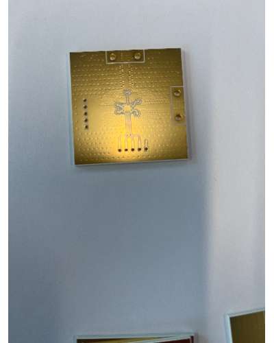
PCBs de RF (Placas de circuito impresso de radiofrequência) são placas de circuito especializadas projetadas para operar em frequências de rádio, normalmente variando de 3 kHz para 300 Ghz. Esses PCBs são essenciais em aplicações que exigem transmissão de sinal precisa e eficiente com perda e distorção mínimas. Este artigo explora as propriedades, estrutura, materiais, processos de fabricação, aplicações, vantagens, e perguntas frequentes (Perguntas frequentes) relacionado a PCBs de RF.
Estrutura de PCBs de RF
A estrutura dos PCBs de RF é meticulosamente projetada para suportar alta frequência integridade e desempenho do sinal:
O substrato é normalmente feito de materiais com baixa constante dielétrica e tangente de perda, como PTFE (Politetrafluoroetileno), Laminados Rogers, ou compósitos de PTFE preenchidos com cerâmica. Esses materiais ajudam a minimizar a perda de sinal e garantem desempenho estável em altas frequências.
Finas camadas de cobre ou outros metais condutores são usadas para traços, garantindo perda mínima de sinal e desempenho de alta frequência. Essas camadas são frequentemente gravadas com precisão para formar os padrões de circuito necessários.
Materiais dielétricos de alto desempenho são usados para separar camadas condutoras, mantendo o isolamento elétrico e a integridade do sinal. Essas camadas são cruciais para evitar interferência de sinal e interferência entre traços adjacentes.
Planos terrestres dedicados fornecem um plano de referência para sinais, reduzindo a interferência eletromagnética (EMI) e melhorando a qualidade do sinal. Os planos terrestres também desempenham um papel vital no gerenciamento térmico, dissipando o calor gerado por operações de alta frequência..
Interconexões verticais conectam diferentes camadas do PCB, permitindo roteamento complexo e projetos de alta densidade. Microvias, em particular, são usados em interconexão de alta densidade (HDI) projetos para minimizar a indutância e capacitância parasitas.
Revestimentos protetores como ENIG (Ouro de imersão em níquel eletrolítico) ou OSP (Conservantes orgânicos de soldabilidade) são usados para melhorar a soldabilidade e proteger contra a oxidação. Esses acabamentos também ajudam a garantir conexões elétricas confiáveis.
Materiais usados em PCBs de RF
Os principais materiais usados em PCBs de RF incluem:
Um material dielétrico de baixa perda conhecido por seu excelente desempenho e estabilidade em alta frequência. O PTFE é frequentemente usado em aplicações que exigem atenuação mínima de sinal e alta integridade de sinal.
Laminados de alto desempenho com baixa constante dielétrica e tangente de perda, projetado especificamente para aplicações de RF e microondas. Os materiais Rogers são preferidos por suas propriedades elétricas consistentes e confiabilidade em altas frequências.
Esses materiais oferecem um equilíbrio de baixa perda, alta condutividade térmica, e estabilidade mecânica. Eles são frequentemente usados em aplicações onde o gerenciamento térmico e a robustez mecânica são críticos.
O cobre de alta pureza é usado para traços condutores devido à sua excelente condutividade elétrica e confiabilidade. A baixa resistência do cobre ajuda a manter a integridade do sinal em altas frequências.
Materiais com baixa constante dielétrica e tangente de perda, como Teflon (Ptfe) e materiais Rogers especializados, são usados para garantir perda e distorção mínimas de sinal. Esses materiais são cruciais para manter a alta qualidade do sinal.
Processo de fabricação de PCBs RF
O processo de fabricação de PCBs de RF envolve várias etapas precisas para garantir desempenho e confiabilidade de alta frequência:
Escolha de materiais de base e camadas condutoras apropriadas com base nos requisitos de desempenho. O processo de seleção considera fatores como constante dielétrica, tangente de perda, propriedades térmicas, e força mecânica.
Empilhar e unir múltiplas camadas de materiais condutores e dielétricos sob condições controladas para formar uma PCB estável. Este processo garante espessura e alinhamento consistentes da camada.
Perfuração de precisão para criar vias e microvias para interconexões verticais entre camadas. Técnicas avançadas de perfuração a laser são frequentemente usadas em microvias para obter alta precisão e danos mínimos aos materiais circundantes.
Galvanoplastia de cobre no substrato e dentro das vias para estabelecer conexões elétricas confiáveis. Esta etapa garante vias fortes e condutoras para transmissão de sinal.
Usando fotolitografia e gravação química para definir os padrões de circuito e interconexões. A padronização precisa é essencial para alcançar o layout e o desempenho do circuito desejados.
Aplicação de revestimentos protetores em superfícies de cobre expostas para melhorar a soldabilidade e proteger contra oxidação. Os acabamentos de superfície também ajudam a prevenir a corrosão e garantem confiabilidade a longo prazo.
Fixação de componentes usando técnicas de soldagem adequadas para aplicações de alta frequência, garantindo perda e distorção mínimas de sinal. O processo de montagem inclui posicionamento cuidadoso e soldagem de componentes de RF para manter a integridade do sinal.
Testes rigorosos de desempenho elétrico, integridade do sinal, e adesão às especificações de design. O teste inclui medições de perda de sinal, verificações de impedância, e ciclagem térmica para garantir confiabilidade sob condições operacionais.
Aplicações de PCBs RF
PCBs de RF são usados em uma ampla gama de aplicações de alta frequência, incluindo:
Estações base, antenas, e módulos RF para redes de comunicação móveis e sem fio. PCBs de RF são essenciais para transmissão e recepção de sinais de alta frequência em sistemas de comunicação.
Sistemas de radar de alta frequência usados na defesa, Aeroespacial, e aplicativos automotivos. PCBs de RF permitem processamento e transmissão precisos de sinais em sistemas de radar.
Equipamentos de diagnóstico e imagem, como máquinas de ressonância magnética e ultrassom, que requerem processamento de sinal de alta frequência. PCBs RF garantem transmissão de sinal precisa e confiável em dispositivos médicos.
Transponders, receptores, e transmissores usados em sistemas de comunicação via satélite. PCBs de RF suportam links de comunicação de alta frequência em sistemas de satélite.
Sensores de alta frequência e sistemas de controle usados em ambientes de fabricação e controle de processos. PCBs RF permitem processamento de sinal confiável e eficiente em automação industrial.
Vantagens dos PCBs RF
RF PCBs oferecem várias vantagens significativas:
Projetado para suportar frequências de RF com mínima perda e distorção de sinal. PCBs de RF garantem alta integridade de sinal e desempenho em altas frequências.
Mantém a qualidade e integridade do sinal através do uso de materiais de baixa perda e processos de fabricação precisos. PCBs de RF minimizam a atenuação e interferência do sinal.
A construção e os testes robustos garantem desempenho e confiabilidade de longo prazo em aplicações exigentes de alta frequência. Os PCBs de RF são construídos para suportar condições operacionais adversas.
Dissipação eficaz de calor através de materiais de substrato e recursos de design, garantindo operação estável sob condições de alta potência. PCBs RF evitam superaquecimento e danos térmicos.
Adequado para uma ampla gama de aplicações de alta frequência em vários setores. PCBs de RF podem ser personalizados para atender a requisitos específicos de design e desempenho.
Perguntas frequentes
Quais materiais são normalmente usados para PCBs de RF, e por que?
PCBs de RF geralmente usam materiais como PTFE, Laminados Rogers, e compósitos de PTFE preenchidos com cerâmica por sua baixa constante dielétrica, tangente de baixa perda, e estabilidade de alta frequência. Esses materiais são essenciais para manter a integridade e o desempenho do sinal.
Como os PCBs de RF diferem dos PCBs padrão?
Os PCBs de RF são projetados especificamente para aplicações de alta frequência, usando materiais especializados e processos de fabricação para minimizar a perda e distorção do sinal. PCBs padrão são normalmente usados para aplicações de baixa frequência e podem não exigir características de desempenho tão rigorosas.
Quais indústrias se beneficiam mais com o uso de PCBs de RF?
Indústrias como telecomunicações, aeroespacial e defesa, dispositivos médicos, Comunicações de satélite, e a automação industrial se beneficiam significativamente do uso de PCBs de RF devido ao seu desempenho e confiabilidade de alta frequência.
Como os PCBs de RF são testados para garantir confiabilidade?
PCBs de RF passam por processos de testes rigorosos, incluindo testes elétricos para integridade e desempenho do sinal, ciclagem térmica, e testes de confiabilidade. Esses testes garantem que os PCBs de RF atendam aos rigorosos padrões de desempenho e durabilidade de alta frequência.