CO., LTD")
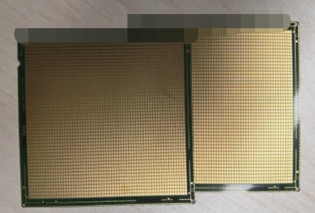
Fabricante de PCB RF, Produção de placas de circuito impresso de alta frequência de rádio. Placas de circuito impresso de radiofrequência (PCBs de RF) são emocionantes, setor em rápido crescimento do Fabricação de placas de circuito impresso indústria. Eles também são incrivelmente complexos, com uma gama estonteante de opções. Os engenheiros da empresa Alcanta PCB podem auxiliá-lo em todas as etapas do processo de fabricação e montagem, incluindo seleção de materiais e chave RF PCB desafios de fabricação para estar ciente.
O que é uma placa de circuito RF? Em termos gerais, a indústria de PCB considera uma placa de circuito de RF qualquer PCB de alta frequência que opera acima de 100 MHz. Dentro da classe de radiofrequência, qualquer coisa acima de 2 GHz é um PCB de micro-ondas.
O que é um PCB de micro-ondas? A principal diferença entre placas de circuito de RF e PCBs de micro-ondas está na frequência de rádio em que operam. PCBs de micro-ondas são classificados como qualquer placa de circuito de RF operando acima de 2 GHz. Placas de circuito de RF e PCBs de micro-ondas são usadas para sinais de comunicação em qualquer aplicação que exija recepção e transmissão de sinais de rádio. Por exemplo, algumas aplicações comuns são telefones celulares e instalações de radar.
PCB de microondas e circuitos de RF – problemas e soluções comuns
Placas de circuito RF, e PCBs de microondas, são especialmente difíceis de projetar em comparação com layouts de PCB tradicionais. Isto se deve aos problemas que podem surgir na recepção ou transmissão dos sinais de rádio. Alguns dos principais problemas são a sensibilidade ao ruído, e tolerâncias de impedância mais rigorosas. Em comparação com placas de circuito tradicionais, sinais de rádio e micro-ondas são muito sensíveis ao ruído e também exigem tolerâncias de impedância muito mais rigorosas. A melhor solução para estes problemas é utilizar plantas baixas e usar um raio de curvatura generoso em traços controlados por impedância.. Em última análise, essas soluções permitirão que o PCB de RF/Microondas alcance o melhor desempenho.
Aplicações de placa RF:As placas RF têm uma infinidade de aplicações diferentes, incluindo tecnologias sem fio, telefones inteligentes, sensores, robótica e segurança. Com o advento de novas tecnologias que estão ultrapassando os limites da eletrônica, a demanda por placas de RF está aumentando.
MATERIAIS DE RF POR APLICAÇÃO: Podemos ajudar em tudo, desde economia de custos em uma placa simples até consultoria de fabricação para peças de última geração., 100 designs de camadas. Para simplificar sua pesquisa, aqui estão várias recomendações para materiais com base na aplicação e capacidade de fabricação:
Nota importante: Dentro de cada setor, existe uma ampla gama de aplicações, demandas, e orçamentos. Temos muitos tipos de materiais de RF em estoque. Para encontrar os melhores materiais de PCB para o seu projeto específico, entre em contato com nossa equipe de engenharia. Nosso e -mail: info@alcantapcb.com
O que é PCB RF?
PCB RF, ou radiofrequência (RF) placa de circuito, é uma placa de circuito especialmente projetada para lidar com sinais de radiofrequência. No campo de alta tecnologia de hoje, a demanda por RF PCB em comunicações sem fio, radar, comunicações por satélite e outros campos estão crescendo dia a dia, tornando-o um dos componentes-chave indispensáveis em equipamentos eletrônicos.
Comparado com PCB tradicional, RF PCB tem diferenças significativas na seleção de materiais, layout e design. Primeiro, PCBs de RF geralmente usam materiais de alta frequência com características específicas, como PTFE (Politetrafluoroetileno) materiais de matriz, e outros materiais compósitos de baixa constante dielétrica e baixa perda. Esses materiais podem fornecer menor atenuação de sinal e interferência cruzada em ambientes de alta frequência, garantindo assim a estabilidade e confiabilidade da transmissão do sinal.
Segundo, existem alguns princípios-chave que o RF PCB precisa seguir quando se trata de layout e design. O layout deve minimizar o comprimento do caminho do sinal para reduzir a atenuação e reflexão do sinal; ao mesmo tempo, evite interseções entre linhas de sinal e linhas de energia ou linhas de terra para reduzir o impacto da diafonia. Além disso, um bom design do plano de aterramento é crucial para RF PCB. O plano de aterramento deve ser tão grande e contínuo quanto possível para fornecer um bom condutor de aterramento e reduzir a impedância do circuito de aterramento. Além disso, a correspondência de impedância também é uma parte importante do projeto para garantir a impedância constante da linha de transmissão de sinal, reduzindo assim a reflexão e a perda do sinal.
Geral, RF PCB tem excelente desempenho e estabilidade em ambientes de alta frequência e é amplamente utilizado em comunicações sem fio, radar, Comunicações de satélite, identificação por radiofrequência (RFID), equipamentos médicos e outros campos. Seu excelente desempenho e confiabilidade fazem dele um componente essencial de muitos dispositivos eletrônicos de última geração., fornecendo uma base sólida para o desenvolvimento da moderna tecnologia de comunicação.
Guia de referência de design de PCB RF.
Existem alguns princípios fundamentais a serem seguidos ao projetar um PCB RF para garantir seu excelente desempenho e estabilidade em ambientes de alta frequência. Aqui estão alguns princípios de design importantes:
Seleção de material
RF PCB geralmente usa materiais específicos de alta frequência, como PTFE (Politetrafluoroetileno) material de matriz. Esses materiais têm baixas constantes dielétricas e baixas perdas, que ajudam a reduzir a atenuação do sinal e a interferência. Ao selecionar materiais, também é necessário considerar sua resistência a altas temperaturas, resistência mecânica e estabilidade química para se adaptar a diferentes ambientes de aplicação.
Local e rota
O layout deve minimizar o comprimento do caminho do sinal para reduzir a perda de sinal e reflexões. Os cruzamentos entre linhas de sinal e linhas de energia ou terra devem ser evitados para reduzir diafonia. Ao mesmo tempo, métodos de fiação razoáveis podem reduzir a interferência eletromagnética (EMI) e interferência de radiofrequência (RFI) e melhorar a capacidade anti-interferência do sistema.
Projeto de planta baixa
Um bom projeto de plano de aterramento é crucial para RF PCB. O plano de aterramento deve ser tão grande e contínuo quanto possível para fornecer um bom condutor de aterramento e reduzir a impedância do circuito de aterramento. Ao otimizar o design do plano terrestre, a resistência e a indutância do circuito de terra podem ser reduzidas, e o caminho atual do fio terra pode ser reduzido, melhorando assim o desempenho e a estabilidade do sistema.
Correspondência de impedância
No projeto de PCB RF, é crucial manter uma impedância constante das linhas de transmissão de sinal para garantir reflexões e perdas mínimas de sinal. Usando tecnologia de correspondência de impedância apropriada, como linhas de microfita, linhas coaxiais, e componentes incorporados, pode efetivamente otimizar a transmissão do sinal e o desempenho do sistema.
Resumindo, projetar RF PCB requer consideração abrangente de fatores-chave, como seleção de material, layout e fiação, projeto do plano terrestre, e correspondência de impedância. Seguir estes princípios de design pode garantir que o RF PCB tenha excelente desempenho e estabilidade, permitindo transmissão confiável de sinal e processamento de dados em ambientes de alta frequência.
Qual material é usado em RF PCB?
O design e desempenho do RF PCB (placa de circuito de radiofrequência) são significativamente diferentes das placas de circuito tradicionais. Uma das diferenças importantes está na escolha dos materiais. Os PCBs de RF geralmente usam materiais específicos com baixa constante dielétrica e baixa perda para garantir excelente desempenho em ambientes de alta frequência. Aqui estão alguns materiais de PCB RF comumente usados:
Ptfe (Politetrafluoroetileno)
PTFE é um dos materiais comumente usados em RF PCB. Possui constante dielétrica extremamente baixa e perda, fazendo-o funcionar bem em ambientes de alta frequência. A estabilidade química e a resistência a altas temperaturas do PTFE também o tornam uma das escolhas ideais para RF PCB.
FR-4
Embora o FR-4 seja um material compósito reforçado com fibra de vidro de uso geral comum, também pode ser usado na fabricação de PCB RF. Dentro de uma faixa de frequência específica, Os materiais FR-4 podem fornecer desempenho satisfatório. No entanto, em frequências mais altas, sua constante dielétrica e perdas causam degradação do desempenho.
Outros materiais compósitos
Além de PTFE e FR-4, existem vários outros materiais compostos que podem ser usados na fabricação de PCB RF. Esses materiais podem ser projetados para faixas de frequência e aplicações específicas, muitas vezes com propriedades personalizadas para atender às necessidades específicas de desempenho.
A aplicação desses materiais em PCBs de RF não apenas transmite efetivamente sinais de radiofrequência, mas também fornece estabilidade, durabilidade e capacidades anti-interferência. Escolhendo os materiais certos, Os projetistas de PCB de RF podem garantir o desempenho e a confiabilidade da placa em ambientes de alta frequência.
Resumindo, PCBs de RF geralmente usam materiais específicos com baixa constante dielétrica e baixa perda, como PTFE, FR-4, e outros materiais compósitos. Esses materiais funcionam bem em ambientes de alta frequência e podem transmitir sinais de RF com eficiência. Selecionando cuidadosamente os materiais, os projetistas podem garantir que os PCBs de RF possam funcionar de maneira ideal em uma variedade de cenários de aplicação.
Qual é o tamanho do RF PCB?
Os PCBs de RF geralmente são dimensionados com base nas necessidades específicas da aplicação, portanto, há vários fatores a serem considerados durante o processo de design. Essas placas podem ser pequenas, adequado para dispositivos móveis portáteis, ou maior, usado em equipamentos maiores, como estações base e sistemas de comunicação.
Para pequenos PCBs RF, como aqueles usados em telefones celulares, equipamento de rede sem fio, ou sensores, as dimensões são geralmente menores para acomodar o design compacto do dispositivo. Essas pequenas placas de circuito geralmente precisam considerar fatores como consumo de energia, dissipação de calor, e restrições de espaço, portanto, seu tamanho pode ser limitado entre alguns centímetros quadrados e dezenas de centímetros quadrados.
Para grandes PCBs de RF, como aqueles usados em equipamentos como estações base, sistemas de comunicação, radares, e comunicações satélites, o tamanho geralmente é maior para acomodar mais componentes eletrônicos e conectores. Essas grandes placas de circuito podem precisar lidar com mais energia, tarefas de transmissão de dados e processamento de sinais, então o tamanho pode atingir dezenas de centímetros quadrados ou até vários metros quadrados.
Quer seja um PCB RF pequeno ou grande, seu tamanho será personalizado de acordo com as necessidades específicas da aplicação. Durante o processo de design, os engenheiros precisam considerar de forma abrangente fatores como a funcionalidade do circuito, Requisitos de desempenho, restrições mecânicas, e custo para garantir que a placa de circuito final possa atender às necessidades do cliente e ter um desempenho ideal em aplicações práticas.
Portanto, PCBs RF vêm em vários tamanhos, dependendo de seus usos e requisitos específicos em diferentes áreas de aplicação. Quer seja um PCB RF pequeno ou grande, seu projeto e fabricação exigem processos precisos e rigoroso controle de qualidade para garantir que possa funcionar de forma estável e confiável em ambientes de alta frequência.
O processo de fabricante de RF PCB.
O processo de fabricação de PCB RF tem muitas semelhanças com a fabricação tradicional de PCB, mas também existem algumas diferenças importantes. Como o RF PCB precisa manter um desempenho estável em ambientes de alta frequência, o processo de fabricação requer um controle de processo mais rígido e maior precisão. A seguir estão as principais etapas no processo de fabricação de RF PCB:
Seleção de material
Ao fabricar PCBs RF, A seleção de material é crucial. Materiais específicos com baixa constante dielétrica e baixas perdas são frequentemente usados, como politetrafluoretileno (Ptfe) materiais de matriz. Esses materiais fornecem bom desempenho de transmissão de sinal em altas frequências e reduzem a atenuação e perda de sinal.
Design Gráfico
O design gráfico do RF PCB é uma das etapas principais no processo de fabricação. Os engenheiros de projeto precisam considerar os caminhos das linhas de sinal, projeto do plano terrestre, correspondência de impedância e outros fatores para garantir que a placa de circuito possa fornecer desempenho estável em ambientes de alta frequência.
Gravura química
Assim que o design estiver concluído, A fabricação de PCB RF normalmente envolve gravação química para criar os padrões de circuito necessários. A gravação química é feita cobrindo uma placa de circuito com uma folha de cobre que foi coberta com um fotossensibilizador., e, em seguida, usando uma solução química para remover as peças indesejadas para formar o padrão de circuito desejado.
Depósito de metal
Após a conclusão do ataque químico, o próximo passo é depositar metal na placa de circuito. O metal comumente usado é o cobre, que fornece boa condutividade elétrica e soldabilidade para garantir a estabilidade e confiabilidade da placa de circuito.
Teste Final
Após a conclusão da fabricação, o RF PCB precisa passar por testes finais para garantir que funcione dentro das especificações. Isso inclui testes completos e verificação da conectividade do circuito, correspondência de impedância, e desempenho de transmissão de sinal. Somente as pranchas que passarem no teste final serão consideradas qualificadas.
Para resumir, o processo de fabricação de PCB RF inclui etapas importantes, como seleção de material, desenho de padrão, gravura química, deposição de metal, e testes finais. O controle rigoroso do processo e os processos de fabricação de alta precisão garantem que o RF PCB tenha excelente desempenho e estabilidade em ambientes de alta frequência.
A área de aplicação do RF PCB.
PCB RF, como uma placa de circuito especialmente projetada para processar sinais de radiofrequência, tem uma ampla gama de aplicações no campo da tecnologia atual. Suas capacidades confiáveis de transmissão de sinais e processamento de dados permitem que ele desempenhe um papel fundamental em vários campos.
Comunicação sem fio
No campo da comunicação sem fio, RF PCB é amplamente utilizado em equipamentos de comunicação móvel, estações base e equipamentos de rede. Através de design otimizado e desempenho de alta frequência, eles alcançam transmissão de sinal estável, suporta vários padrões de comunicação, como LTE, 5G, etc., e fornecer às pessoas serviços de comunicação sem fio confiáveis e de alta velocidade.
Comunicações por satélite
As comunicações por satélite são métodos de comunicação que transmitem informações através de satélites para o solo ou outros locais. RF PCB desempenha um papel vital em sistemas de comunicação via satélite e é usado em transmissores, receptores e sistemas de antenas de equipamentos de comunicação via satélite para garantir transmissão estável e processamento eficiente de sinais.
Radar
Sistemas de radar são usados para detectar, rastrear e identificar alvos, e são amplamente utilizados na aviação, militares, previsão do tempo e outros campos. RF PCB é usado na transmissão de sinal, módulos de recepção e processamento no sistema de radar. Através de controle e processamento preciso de sinal, o alto desempenho e alta confiabilidade do sistema de radar são alcançados.
Identificação por radiofrequência (RFID)
A tecnologia RFID realiza a identificação e rastreamento de objetos através de sinais de radiofrequência e é amplamente utilizada na gestão logística, gestão de armazenamento, transporte inteligente e outros campos. Como um componente chave do leitor RFID e do sistema de antena, RF PCB suporta a identificação e troca de dados de tags RFID, permitindo aplicações IoT eficientes.
Equipamento Médico
Na área médica, RF PCB é usado em aplicações como equipamentos de diagnóstico médico, equipamento de monitoramento sem fio, e transmissão de imagens médicas. Eles permitem a operação eficiente e o diagnóstico preciso de equipamentos médicos por meio de processamento de sinais e transmissão de dados de alta precisão, fornecendo suporte importante para cuidados médicos.
Resumindo, RF PCB desempenha um papel insubstituível nas comunicações sem fio, Comunicações de satélite, radar, identificação por radiofrequência (RFID), equipamentos médicos e outros campos. Suas capacidades confiáveis de transmissão de sinal e processamento de dados fornecem suporte fundamental para aplicações em todas as esferas da vida, promover o avanço contínuo da ciência e da tecnologia e a expansão contínua das aplicações.
Quais são as vantagens do RF PCB?
Os PCBs de RF oferecem muitas vantagens significativas em relação aos projetos de circuitos tradicionais, o que os torna ideais para muitas aplicações de alta frequência..
Em primeiro lugar, O design do RF PCB é especificamente para sinais de alta frequência, para que possa fornecer transmissão de sinal mais estável e confiável. Em ambientes de alta frequência, transmissão de sinal enfrentará mais desafios, como atenuação de sinal, reflexão, e interferência. Usando materiais específicos de alta frequência, layout e design precisos, RF PCB pode efetivamente superar esses problemas e garantir uma transmissão de sinal estável.
Segundo, RF PCB usa materiais de baixa perda e design otimizado, o que pode reduzir significativamente a perda e atenuação do sinal. Em ambientes de alta frequência, a perda de sinal será mais significativa, portanto, o uso de materiais de baixa perda é crucial para manter a força do sinal. O design do RF PCB não considera apenas a seleção de materiais, mas também otimiza os métodos de fiação e conexão para minimizar a perda de sinal.
Além disso, o design do RF PCB leva em consideração o desempenho anti-interferência, o que pode efetivamente reduzir o impacto da interferência externa no sinal. Em ambientes de alta frequência, interferência externa pode vir de várias fontes, como outros equipamentos eletrônicos, radiação eletromagnética, etc.. RF PCB pode resistir eficazmente a essas interferências e garantir a pureza e estabilidade do sinal, adotando medidas de blindagem, bom design de plano terrestre, e correspondência de impedância.
Resumindo, RF PCB tem vantagens óbvias em aplicações de alta frequência, incluindo transmissão de sinal mais estável, menor perda de sinal e maior capacidade anti-interferência. Essas vantagens tornam o RF PCB a primeira escolha em comunicações sem fio, radar, comunicações por satélite e outros campos, fornecendo soluções de circuito confiáveis para essas aplicações.
Perguntas frequentes
Como o processo de fabricação do PCB RF difere do PCB comum?
O processo de fabricação do PCB RF é semelhante ao do PCB normal em alguns aspectos, mas também existem algumas diferenças importantes. Em primeiro lugar, a seleção do material do RF PCB é muito importante. Geralmente é necessário selecionar materiais de alta frequência com constante dielétrica e fator de perda específicos, como PTFE (Politetrafluoroetileno) matriz. Segundo, o processo de fabricação de PCB RF requer maior precisão e controle do processo para garantir a consistência e estabilidade da placa PCB. Finalmente, no processo de fabricação de RF PCB, a correspondência de impedância e as características da linha de transmissão de sinal são cruciais, exigindo controle e testes de processo mais rigorosos.
O que é correspondência de impedância para RF PCB? Por que é tão importante?
A correspondência de impedância do PCB RF refere-se a garantir que a impedância da linha de transmissão do sinal no PCB corresponda à impedância do dispositivo conectado ou outro circuito. A correspondência de impedância é crítica para minimizar reflexões e perdas de sinal. Se a impedância de uma linha de transmissão de sinal não corresponder à impedância do dispositivo conectado, reflexões de sinal, perda de energia, e a degradação do desempenho resultará.
Como o RF PCB lida com a interferência eletromagnética (EMI) problemas?
O projeto de PCB RF precisa considerar a interferência eletromagnética (EMI) questões para garantir que tenha boas capacidades anti-interferência em ambientes de alta frequência. Alguns métodos comuns incluem um bom projeto de plano de terra, uso de escudos, layout e roteamento da linha de sinal, etc.. Além disso, a seleção de materiais de PCB apropriados e o controle rigoroso do processo também podem ajudar a reduzir a interferência eletromagnética.
Quais fatores especiais precisam ser considerados no projeto de RF PCB?
O projeto de PCB RF precisa considerar muitos fatores especiais, incluindo características de transmissão de sinais de alta frequência, correspondência de impedância, perda de sinal, projeto do plano terrestre, Supressão EMI, layout e fiação, etc.. Comparado com o design tradicional de PCB, O design de PCB RF requer maior precisão e controle de processo mais rigoroso para garantir seu desempenho estável e confiável em ambientes de alta frequência.