CO., LTD")
Devis de substrat semi-conducteur BGA. Matériau haute vitesse et haute fréquence substrat d'emballage fabrication. Substrat d'emballage avancé.
Dans le domaine dynamique d’aujourd’hui PCB ingénierie, réseau de grilles à billes à semi-conducteurs (BGA) les substrats sont devenus des composants indispensables et critiques pour l'installation et l'interconnexion d'éléments électroniques, en raison de leur design distinctif et de leurs performances exceptionnelles. Cet article approfondit une analyse complète du substrat semi-conducteur BGA, dévoilant son rôle central et ses attributs uniques au sein des PCB.
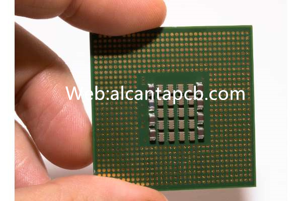
Le substrat semi-conducteur BGA, une abréviation pour substrat Ball Grid Array, joue un rôle crucial dans la conception des PCB. Servir de composant central pour connecter et monter des éléments électroniques, il agit comme un intermédiaire vital entre la puce semi-conductrice et l'ensemble du PCB. Ceci est réalisé grâce à son réseau de grilles à billes distinctif (BGA) configuration, permettant des connexions électriques efficaces.
Contrairement aux connexions à broches traditionnelles, le BGA utilise des billes de soudure sphériques pour établir des connexions. Cette conception augmente non seulement la densité de connexion, mais améliore également la dissipation thermique. L'adoption de cette configuration confère au substrat semi-conducteur BGA d'excellentes performances électriques et fiabilité..
Le substrat semi-conducteur BGA agit comme un pont dans la connexion et l'installation des composants électroniques. Au-delà de fournir une connexion électrique fiable, il offre un moyen efficace de dissiper la chaleur de la puce. Cette conception rend les substrats semi-conducteurs BGA largement applicables dans les appareils électroniques hautes performances et densément configurés..
En raison de ses performances exceptionnelles, semiconductor BGA substrates find extensive use in electronic equipment across various industries. From consumer electronics to automobiles and medical equipment, semiconductor BGA substrates are ubiquitous. Their versatility and reliability make them integral components of contemporary electronic designs.
With its unique design and outstanding performance, the semiconductor BGA substrate has become an indispensable key player in modern electronic design. It revitalizes the performance and reliability of electronic devices by serving as a bridge between the semiconductor chip and the entire PCB, while promoting efficient electrical connections through ball grid array configurations. In the future of the electronic field, semiconductor BGA substrates are poised to maintain a decisive role, leader de la tendance de l'innovation dans la conception électronique.
Quels sont les types de substrats semi-conducteurs BGA?
Dans l'ingénierie contemporaine des PCB, réseau de grilles à billes à semi-conducteurs (BGA) les substrats ont suscité un intérêt considérable en raison de leur conception distinctive et de leurs applications polyvalentes. Cet article explorera la diversité des substrats semi-conducteurs BGA, avec un accent particulier sur deux types cruciaux: Interconnexion haute densité (HDI) et substrats organiques.
Ce type de substrat permet des performances électriques supérieures en permettant davantage d'interconnexions dans un espace limité. Le substrat HDI utilise une technologie de stratification avancée pour empiler plusieurs couches de circuits imprimés, réduisant ainsi la taille globale.
La conception spéciale du substrat HDI le rend adapté à de nombreuses applications haut de gamme, tels que les appareils mobiles et les équipements de communication. Ses principales caractéristiques comprennent:
Interconnexion haute densité (HDI) les substrats présentent un design distinctif qui facilite un nombre accru de connexions dans des espaces confinés, presenting an optimal solution for intricate circuits.
The miniaturization capability of HDI substrates, achieved through lamination technology, allows for reduced sizes while maintaining high performance, rendering them highly suitable for slim and lightweight electronic devices.
HDI substrates significantly enhance electrical performance by shortening signal transmission paths and reducing resistance and inductance, en particulier dans les applications haute fréquence.
D'autre part, substrats organiques, another vital type of semiconductor BGA substrate, employ materials like glass fiber and resin in their preparation process. These substrates demonstrate outstanding performance across a broad range of application scenarios.
The simplicity of the preparation process for organic substrates affords them flexibility in diverse application scenarios. Their cost-effectiveness, often surpassing that of high-end materials, makes them particularly well-suited for high-volume production.
Organic substrates find widespread application in various fields, y compris l'électronique grand public, électronique automobile, et matériel de communication.
The diversity of semiconductor BGA substrates provides a wide range of choices for electronic designs. HDI and organic substrates meet the needs of different design requirements and application fields with their unique characteristics. Design engineers can take full advantage of these substrate types according to project needs, thereby promoting innovation and development of electronic technology.
Quels sont les avantages du substrat semi-conducteur BGA?
The Semiconductor Ball Grid Array (BGA) substrate has emerged as a transformative element in contemporary PCB engineering, ushering in significant advancements in electronic design and manufacturing. Its exceptional electrical performance, capacités de miniaturisation, et une gestion thermique supérieure en font un pionnier en matière d'innovation dans les appareils électroniques. Approfondir, Explorons les avantages des substrats semi-conducteurs BGA et leur rôle central dans l'amélioration des performances globales des appareils électroniques.
Avec configuration BGA, ces substrats fournissent des connexions électriques plus denses et plus fiables. La conception du réseau de grilles à billes augmente non seulement la densité de connexion, mais réduit également la résistance et l'inductance de la transmission du signal, résultant en des performances électriques plus stables et efficaces. Cet avantage en termes de performances est essentiel pour les applications avec des fréquences élevées et des débits de transmission de données élevés., fournir un environnement de transmission de signal fiable pour les appareils électroniques.
L'avantage unique des substrats semi-conducteurs BGA réside dans leurs capacités de miniaturisation exceptionnelles dans la conception électronique.. La configuration BGA permet d'accueillir un plus grand nombre de broches sur le substrat, facilitant une disposition plus compacte des composants électroniques. Cette conception miniaturisée contribue non seulement à la réduction globale de la taille des appareils électroniques, mais offre également une flexibilité de conception améliorée.. Dans le domaine des appareils mobiles modernes, écouteurs, et autres produits électroniques compacts, les capacités de miniaturisation des substrats semi-conducteurs BGA constituent un moteur essentiel de l'innovation.
Les réseaux à billes configurés avec BGA présentent des avantages en termes de conductivité thermique, aidant à disperser et à transférer la chaleur plus efficacement. Ceci est essentiel pour les appareils électroniques qui gèrent des composants de forte puissance et fonctionnent pendant de longues périodes., s'assurer que l'appareil fonctionne dans une plage de température stable, augmentation de la fiabilité et de la longévité.
L'effet combiné de ces avantages contribue de manière significative à l'efficacité globale des appareils électroniques.. Des performances électriques supérieures garantissent une transmission fiable du signal, les capacités de miniaturisation entraînent une réduction de la taille des appareils, et une gestion thermique supérieure améliore la stabilité et la fiabilité de l'appareil.
Les substrats semi-conducteurs BGA ont insufflé une nouvelle vague d'énergie dans l'évolution des appareils électroniques, en raison de leurs performances électriques exceptionnelles, capacités de miniaturisation, et une gestion thermique efficace. Avec leur design et leurs fonctionnalités innovantes, ils sont devenus un composant essentiel de l'ingénierie moderne des PCB, établir une base solide pour les progrès continus dans l'industrie électronique.
Pourquoi choisir un substrat semi-conducteur BGA?
Dans la conception et la fabrication électroniques contemporaines, l'adoption du Ball Grid Array à semi-conducteurs (BGA) les substrats représentent plus qu’une simple tendance dominante; cela vient de leur performance exceptionnelle, utilisation efficace de l'espace, et adaptabilité aux technologies de pointe. Contrairement aux circuits imprimés classiques (PCBS), Les substrats semi-conducteurs BGA présentent des avantages remarquables et offrent des solutions distinctives dans divers scénarios d'application..
Les substrats semi-conducteurs BGA se distinguent par leurs excellentes propriétés électriques. Par rapport aux PCB traditionnels, sa structure de conception permet aux composants électroniques d'être plus étroitement intégrés, réduisant les chemins de transmission du signal et améliorant la stabilité et la fiabilité du circuit. Ceci est particulièrement critique pour les scénarios d'application qui nécessitent des performances élevées., such as communication equipment and computer systems.
Avec la tendance des équipements électroniques modernes à rechercher une taille plus petite, le substrat semi-conducteur BGA permet aux composants d'être disposés plus étroitement sur le substrat grâce à son ensemble unique de grilles à billes (BGA) configuration. Cette disposition compacte améliore non seulement l'intégration des composants, mais réduit également efficacement la taille de l'appareil global. Cette amélioration de l'utilisation de l'espace est essentielle pour les, lumière, appareils portables tels que smartphones et tablettes.
La conception des substrats semi-conducteurs BGA rationalise considérablement l'intégration transparente des technologies avancées. Son interconnexion haute densité (HDI) la conception simplifie l'incorporation de composants électroniques de plus en plus complexes, répondre aux exigences d’une technologie en évolution rapide. As fields like the Internet of Things and artificial intelligence continue to expand, semiconductor BGA substrates demonstrate enhanced capabilities to effectively tackle burgeoning technical challenges.
Taking high-end communication equipment as an example, network routers using semiconductor BGA substrates can be smaller and lighter than traditional PCB routers with the same performance. This not only saves space, but also improves the heat dissipation effect of the device, further improving overall performance.
Dans l'ensemble, the excellent performance, space utilization and adaptability to advanced technologies of semiconductor BGA substrates make it the first choice in modern electronic design. Its wide application in various industries demonstrates the irreplaceability of this technology. When choosing electronic component substrates, Les substrats semi-conducteurs BGA constituent sans aucun doute un choix judicieux pour les applications axées sur les performances et l'espace..
Comment fabriquer un substrat semi-conducteur BGA?
Le processus de fabrication du substrat semi-conducteur BGA est un élément essentiel de l’ingénierie électronique, impliquant la production de cartes mères et de substrats. Ci-dessous, nous explorons en détail ce processus de fabrication complexe et sophistiqué., y compris les étapes clés, matériaux utilisés et utilisation de technologies avancées.
Dans la fabrication de cartes mères, une analyse approfondie des processus de fabrication soustractive et additive est une étape cruciale pour comprendre l’ensemble du processus de production. Cette étape comprend des étapes pour découper la forme de la carte mère et ajouter des composants supplémentaires. L'utilisation de matériaux et de technologies avancés est un facteur clé pour garantir d'excellentes performances de la carte mère..
Les étapes de découpe et d'ajout du processus de fabrication ont un impact direct sur la forme finale de la carte mère. Cela implique de couper, façonner et ajouter des composants à la feuille. Grâce à une opération minutieuse, s'assurer que la carte mère répond aux exigences de conception en termes de forme et de fonction.
L'utilisation de matériaux avancés, comme les composites haute performance, détient le potentiel d’améliorer à la fois la résistance et la conductivité thermique des cartes mères. Intégrer des technologies de fabrication avancées, comme la découpe laser précise et la robotique automatisée pour l'intégration de composants, améliore non seulement l'efficacité de la fabrication, mais garantit également la précision de la production.
La fabrication de substrats est un autre maillon clé du processus de fabrication des substrats semi-conducteurs BGA.. Une attention particulière est accordée au rôle de la technologie d'interconnexion haute densité et aux matériaux utilisés centrés sur la configuration BGA., ce qui constitue une étape importante pour garantir les performances supérieures des substrats semi-conducteurs BGA.
L’objectif principal du Ball Grid Array (BGA) la configuration consiste à établir des interconnexions haute densité reliant les puces à la carte mère via des réseaux de billes. L'évolution de cette technologie a permis l'intégration d'un plus grand nombre de points de connexion dans un espace compact, améliorant ainsi la complexité du circuit et les performances globales.
Dans la fabrication de substrats, la sélection de matériaux performants, notamment FR-4 et polyimide, est crucial. FR-4 excelle en fournissant des propriétés d’isolation électrique exceptionnelles, tandis que le polyimide démontre une résistance exceptionnelle aux températures élevées, ce qui le rend bien adapté aux environnements opérationnels exigeants des équipements électroniques complexes.
Grâce à l'ingénieuse combinaison de ces étapes clés et de ces matériaux, le processus de fabrication des substrats semi-conducteurs BGA devient une prouesse technologique dans l’ingénierie électronique moderne. L'innovation et l'optimisation continues de ce processus de fabrication constituent une base solide pour l'amélioration des performances et la réduction de la taille des appareils électroniques..
Quelles sont les applications des substrats semi-conducteurs BGA?
Réseau de grilles à billes à semi-conducteurs (BGA) les substrats sont largement utilisés dans l'industrie des équipements médicaux, jouant un rôle crucial dans divers appareils, y compris les moniteurs cardiaques, équipement d'imagerie médicale, et dispositifs médicaux portables. Appréciés pour leur fiabilité et leur stabilité exceptionnelles, ces substrats contribuent à améliorer la précision des équipements, des temps de réponse plus rapides, et des capacités améliorées de traitement des données. Par conséquent, ils contribuent à une expérience médicale globale améliorée pour les patients.
Dans la fabrication de téléphones mobiles, l'intégration de substrats semi-conducteurs BGA contribue à la finesse et à la réduction du poids du dispositif, tout en prenant en charge une transmission et un traitement efficaces des données.
Les substrats semi-conducteurs BGA jouent un rôle crucial dans le domaine des systèmes de conduite intelligents au sein des automobiles en facilitant l'intégration transparente des composants électroniques.. Cette intégration se traduit par des mécanismes de contrôle intelligents et un retour d'information en temps réel pour les véhicules, améliorant finalement la sécurité et la commodité pendant la conduite.
Dans le domaine du matériel médical, l'adoption de substrats semi-conducteurs BGA apporte des améliorations significatives en termes de précision et de fiabilité des équipements. Ce, à son tour, contribue à une précision accrue du diagnostic médical et à une efficacité accrue du traitement.
L'adoption généralisée des substrats semi-conducteurs BGA constitue un moteur fondamental de l'innovation technologique dans diverses industries.. De l’électronique grand public aux appareils automobiles et médicaux, ces substrats polyvalents et fiables répondent non seulement aux exigences rigoureuses des appareils modernes, mais fournissent également un support robuste pour les futurs projets de conception et de fabrication électroniques.. L'évolution continue de cette technologie innovante continuera à propulser les progrès dans diverses industries., ouvrant la voie à une commodité et à des possibilités accrues dans la vie et le travail des gens.
Où trouver un substrat semi-conducteur BGA?
Faites attention aux entreprises réputées dans le domaine de l'ingénierie des PCB. Leurs produits ont tendance à être soumis à un contrôle de qualité strict et à se conformer aux normes de l'industrie.. Ces entreprises possèdent généralement une vaste expérience dans la satisfaction de divers besoins de projets..
Lors de la sélection d'un substrat semi-conducteur BGA, un devis précis est crucial. Assurer une communication claire avec les fournisseurs sur les exigences du projet afin d'obtenir des estimations de coûts précises. Cela permet de planifier votre budget et d'éviter des dépenses inutiles.
Sur le marché concurrentiel d’aujourd’hui, notre entreprise se distingue par sa qualité et son service exceptionnels en tant que fournisseur de confiance de substrats semi-conducteurs BGA. Engagé à répondre aux exigences les plus rigoureuses des clients et à être à la pointe de l’innovation du secteur, nous sommes fiers de nos mesures strictes de contrôle de qualité.
Notre engagement envers un excellent contrôle de qualité se reflète dans notre adhésion à des normes strictes., garantissant que chaque substrat semi-conducteur BGA atteint des performances et une fiabilité maximales. Bénéficiant de plus d'une décennie d'expérience en ingénierie des PCB, notre entreprise navigue facilement dans le paysage dynamique de l'industrie, proposer des solutions pratiques adaptées à l’évolution des besoins.
La satisfaction du client est au cœur de nos opérations, comme l'illustre notre approche de service orientée client. Nous collaborons étroitement avec les clients, comprendre minutieusement les exigences du projet pour fournir des solutions sur mesure qui favorisent leur succès. La transparence et l'exactitude définissent notre processus de devis, répondre aux préoccupations budgétaires grâce à une communication claire et une compréhension globale des détails du projet.
Lors de la sélection d'un fournisseur de substrat semi-conducteur BGA, donner la priorité à ceux qui jouissent d’une excellente réputation et d’une force dans l’industrie. Notre entreprise, avec sa qualité exceptionnelle, une vaste expérience, et un service centré sur le client, se présente comme un partenaire fiable pour les substrats semi-conducteurs BGA. Nous attendons avec impatience l'opportunité de collaborer avec vous pour façonner le brillant avenir de la conception électronique..
Citation du substrat semi-conducteur BGA
Cet article approfondit les considérations nuancées concernant les devis de substrats semi-conducteurs BGA., examiner comment les coûts varient en fonction du type de substrat, complexité, et volume de production. Il encourage les lecteurs à rechercher des devis personnalisés adaptés aux exigences spécifiques de leur projet..
Lors de l'évaluation d'un devis de substrat semi-conducteur BGA, plusieurs facteurs ont un impact significatif sur les coûts. Différents types de substrats, comme l'interconnexion haute densité (HDI) et substrats organiques, sont livrés avec des matériaux et des processus de fabrication distincts qui influencent directement les dépenses. Par exemple, Les substrats HDI entraînent souvent des coûts de fabrication plus élevés mais offrent des performances et une densité supérieures.
La complexité du support est un autre facteur important dans la détermination du devis.. Les conceptions plus complexes nécessitent souvent plus d’étapes de production et une technologie avancée, rendant la fabrication plus difficile et plus coûteuse.
Le volume de production est un facteur clé qui affecte directement les coûts. La production à grande échelle permet souvent d'obtenir des résultats plus économiques car les coûts fixes peuvent être répartis sur un plus grand nombre de produits.. Inversement, la production à petite échelle peut nécessiter des coûts plus élevés.
La cotation du substrat semi-conducteur BGA n’est pas statique, mais est affecté par l’impact global de plusieurs facteurs. Voici les principaux mécanismes de mouvement des prix:
Les matériaux et procédés utilisés dans différents types de substrats varient considérablement, donc leurs coûts de fabrication varieront également considérablement. Les fluctuations des prix des matériaux dans la chaîne d'approvisionnement affecteront également directement le prix final du substrat..
La complexité de la conception aura un impact direct sur le temps et les ressources nécessaires pendant la production. À mesure que la complexité de la conception augmente, les fabricants devront peut-être adopter des équipements et des technologies plus avancés, ce qui augmentera également les coûts.
La production à grande échelle peut réduire la proportion des coûts fixes, réduisant ainsi le coût de fabrication de chaque unité. Donc, les commandes à grande échelle bénéficient généralement de prix plus compétitifs.
Soulignant l'importance d'obtenir des devis personnalisés pour les lecteurs’ besoins uniques du projet. Les devis personnalisés peuvent refléter plus précisément les exigences réelles du projet et garantir que les coûts sont contrôlés dans une fourchette acceptable.. En outre, une communication directe avec les fabricants pour partager les exigences spécifiques du projet peut également contribuer à établir une relation de travail plus étroite et à jeter les bases d'une coopération future.
La cotation du substrat semi-conducteur BGA est une considération globale et est affectée par l'imbrication de plusieurs facteurs. Par une compréhension approfondie des facteurs qui affectent les coûts et du mécanisme de variation des prix, les lecteurs peuvent formuler des stratégies d'approvisionnement de manière plus rationnelle et obtenir un plus grand succès dans les projets. Les lecteurs sont encouragés à profiter de devis personnalisés pour garantir que leur achat de substrats semi-conducteurs BGA répond aux besoins spécifiques de leur projet..
Questions fréquemment posées
Ce qui distingue les substrats semi-conducteurs BGA des PCB traditionnels?
Les substrats semi-conducteurs BGA se distinguent grâce à leur système unique Ball Grid Array. (BGA) configuration, faciliter des connexions électriques efficaces entre les puces semi-conductrices et le PCB plus large. Cette conception distinctive améliore les performances, utilisation de l'espace, et adaptabilité aux technologies de pointe.
Comment les substrats semi-conducteurs BGA contribuent-ils à la miniaturisation?
La conception compacte et les interconnexions haute densité des substrats semi-conducteurs BGA permettent une miniaturisation efficace, un avantage clé dans l’électronique moderne. Cette fonctionnalité est particulièrement bénéfique dans les applications où les contraintes d'espace sont critiques.
Quelles sont les principales considérations à prendre en compte lors du choix entre différents types de substrats semi-conducteurs BGA?
Le processus de sélection implique l'évaluation des exigences de conception spécifiques et des besoins d'application.. Interconnexion haute densité (HDI), substrats organiques, et d'autres types offrent des fonctionnalités variées, et le choix dépend de facteurs tels que les exigences de performances et les spécifications du projet.
Où peut-on trouver des sources réputées pour les substrats semi-conducteurs BGA?
Identifier des fabricants et des distributeurs fiables est crucial. Des acteurs réputés du secteur proposent souvent une gamme de substrats BGA pour semi-conducteurs, assurer la qualité et le respect des spécifications requises pour la réussite des projets électroniques.
Comment varie le coût des substrats semi-conducteurs BGA, et quels facteurs influencent les cotations?
Les considérations de coût sont influencées par des facteurs tels que le type de substrat, complexité, et volumes de production. La recherche de devis personnalisés basés sur les exigences du projet est essentielle pour une budgétisation et une planification de projet précises..
Les substrats semi-conducteurs BGA peuvent-ils être personnalisés pour les besoins spécifiques d'un projet?
Oui, Les substrats semi-conducteurs BGA offrent des options de personnalisation pour répondre aux exigences spécifiques du projet. Cette flexibilité est bénéfique pour les projets avec des exigences de conception ou de performances uniques.