CO., LTD")
Semicondutor Substrato BGAFabricante, Produzimos principalmente substrato de pitch bump ultra-pequeno, traço e espaçamento ultrapequenos substrato da embalagem
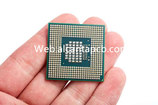
Semicondutor BGA (Matriz de Grade de Bola) substrato é uma tecnologia de empacotamento de alta densidade amplamente utilizada no empacotamento e conexão de circuitos integrados (ICS). Ele usa bolas de solda esféricas como meio de conexão, para que os chips da placa de circuito possam ser conectados à placa-mãe ou outros dispositivos através dessas bolas de solda esféricas. Comparado com embalagens tradicionais baseadas em pinos, Substratos BGA podem atingir maior densidade de conexão e melhor desempenho elétrico.
Os substratos BGA são geralmente feitos de materiais semicondutores, como silício, arseneto de gálio (Gaas), etc.. Sua estrutura consiste em chips, substratos de embalagem, bolas e conectores esféricos de solda. Durante o processo de fabricação, chips são embalados em um substrato e conectados por meio de técnicas de soldagem. Esta tecnologia de empacotamento permite que os substratos BGA tenham maior confiabilidade e melhores recursos de gerenciamento térmico, tornando-os adequados para uma variedade de aplicações de dispositivos eletrônicos de alto desempenho.
As principais características do substrato BGA incluem:
Conexão de alta densidade: Através da tecnologia de conexão de esfera de solda esférica, o substrato BGA pode alcançar conexões de maior densidade, permitindo que mais chips e dispositivos sejam acomodados na placa de circuito.
Excelente desempenho elétrico: O substrato BGA tem um caminho de transmissão de sinal mais curto e menor resistência e indutância, melhorando assim o desempenho e a estabilidade do circuito.
Bom gerenciamento térmico: Devido ao bom contato entre as esferas de solda e o substrato, o substrato BGA pode transferir e dispersar de forma mais eficaz o calor gerado pelo chip, reduzindo o estresse térmico do chip e melhorando a confiabilidade do sistema.
Em geral, O substrato semicondutor BGA é uma tecnologia de embalagem avançada que fornece soluções estáveis e de alto desempenho para o projeto e fabricação de equipamentos eletrônicos. Com o contínuo desenvolvimento e progresso da indústria eletrônica, Os substratos BGA continuarão a desempenhar um papel importante, promovendo a inovação contínua da tecnologia e a expansão das aplicações.
Qual é o processo de fabricação de substratos BGA semicondutores?
O processo de fabricação de substratos BGA semicondutores envolve várias etapas principais, cada etapa é crucial e afeta a qualidade e o desempenho do produto final. Essas etapas principais são detalhadas abaixo:
Projeto: O primeiro passo na fabricação de um substrato BGA semicondutor é o projeto. Nesta fase, o fabricante trabalha com o cliente para determinar as especificações, dimensões, e layout do substrato. A equipe de design usa software CAD para projetar e garantir que o layout da fiação e do conector do substrato atenda aos requisitos do produto.
Seleção de material: A seleção de materiais semicondutores de alto desempenho adequados para uma aplicação específica é uma etapa crítica no processo de fabricação. Esses materiais incluem materiais de substrato, materiais de embalagem, fios metálicos, etc.. Os fabricantes selecionarão materiais apropriados com base nos requisitos do produto e indicadores de desempenho para garantir a estabilidade e confiabilidade do substrato.
Processamento de gráficos e imagens: O fabricante importará a imagem do substrato BGA projetada para o software de processamento gráfico e de imagem, e realizar vários ajustes e otimizações de parâmetros para garantir que a imagem final possa refletir com precisão os requisitos do projeto.
Fotolitografia: Durante o processo de fabricação, a fotolitografia é usada para transferir padrões projetados para a superfície do substrato. A fotolitografia é um processo preciso que utiliza resina fotossensível e fotorresistente para projetar padrões na superfície de um substrato e realizar tratamentos químicos correspondentes para formar o padrão desejado..
Gravura: Depois da fotolitografia, um processo de gravação é necessário para remover partes indesejadas do material da superfície do substrato, deixando os padrões e conectores desejados. A gravação pode usar métodos como gravação química ou gravação física, e o processo de gravação apropriado pode ser selecionado de acordo com diferentes materiais e requisitos de design.
Metalização: Após a conclusão da gravação, a superfície do substrato precisa ser metalizada para melhorar o desempenho condutor do conector. A metalização pode usar métodos como galvanoplastia ou deposição química de vapor para depositar uma camada de metal na superfície de um substrato para formar um conector condutor.
Embalagem: Embalagem é o processo de montagem de um chip de circuito integrado em um substrato BGA. Os fabricantes utilizam equipamentos sofisticados para unir os chips ao substrato e mantê-los no lugar com soldagem ou outros métodos de fixação.. O processo de embalagem também inclui etapas como instalação de um dissipador de calor e preenchimento da cola de embalagem para melhorar a estabilidade e o desempenho de dissipação de calor do chip.
Testes e controle de qualidade: A última etapa crítica são testes rigorosos e controle de qualidade do substrato BGA fabricado. Os fabricantes usam vários equipamentos e métodos de teste para testar o desempenho dos substratos e garantir que atendam aos requisitos e padrões do produto. Somente substratos que passem no teste podem ser entregues aos clientes para uso.
Resumindo, o processo de fabricação de substratos BGA semicondutores inclui várias etapas importantes, como design, Seleção de material, processamento de gráficos e imagens, fotolitografia, gravura, metalização, embalagem, testes e controle de qualidade. Cada etapa requer equipamentos sofisticados e suporte técnico para garantir que a qualidade e o desempenho do produto final atendam aos requisitos e expectativas do cliente..
Quais são as vantagens dos substratos BGA semicondutores em comparação com outros substratos?
Substratos semicondutores BGA têm muitas vantagens sobre outros substratos, o que os torna uma das tecnologias de embalagem preferidas no campo da eletrônica atual.
Primeiro, o substrato semicondutor BGA tem maior densidade. O substrato BGA usa tecnologia de conexão de grade de esferas. Comparado com métodos de embalagem tradicionais, seus pontos de conexão são mais densos, para que possa acomodar mais conectores e chips em um espaço limitado. Isso torna os substratos BGA ideais para implementar projetos de circuitos integrados de alta densidade, especialmente para pequenos dispositivos eletrônicos e aplicações de alto desempenho.
Segundo, o substrato BGA possui desempenho elétrico superior e características de transmissão de sinal. Devido à adoção da tecnologia de conexão de matriz de grade esférica, Substratos BGA podem fornecer caminhos de sinal mais curtos e menor resistência e indutância, reduzindo assim o atraso e a perda do sinal, e melhorando a estabilidade e confiabilidade da transmissão de sinal. Isto é particularmente importante para aplicações que exigem transmissão de dados em alta velocidade e baixo consumo de energia., como equipamentos de comunicação, computadores e eletrônicos de consumo.
Além disso, substratos semicondutores BGA têm melhores propriedades de gerenciamento térmico. O design do substrato BGA permite dispersar e dissipar de forma mais eficaz o calor gerado pelo chip, reduzindo assim a temperatura do sistema e melhorando a eficiência da dissipação de calor. Isto é fundamental para chips de alto desempenho e dispositivos de longa duração para garantir a estabilidade e confiabilidade do sistema.
Além disso, Os substratos BGA também apresentam maior confiabilidade e resistência ao impacto. Porque seu método de soldagem é mais confiável e os pontos de conexão são encapsulados sob o substrato por uma grade esférica, pode resistir melhor a choques mecânicos e vibrações, reduzindo a desconexão ou danos causados por fatores ambientais externos. Isso torna os substratos BGA amplamente utilizados em áreas como controle industrial, eletrônica automotiva, e aeroespacial, onde o equipamento tem requisitos extremamente elevados de confiabilidade e durabilidade.
Resumindo, o substrato semicondutor BGA tem muitas vantagens, como maior densidade, desempenho elétrico superior, melhor desempenho de gerenciamento térmico e maior confiabilidade do que outros substratos. Estas vantagens tornam os substratos BGA a solução de embalagem preferida para vários dispositivos eletrônicos, impulsionando o desenvolvimento contínuo e o progresso da indústria eletrônica.
Em quais campos os substratos BGA semicondutores são usados?
Substratos semicondutores BGA são amplamente utilizados no campo da tecnologia moderna e desempenham um papel importante em vários campos. A seguir estão várias áreas principais de aplicações de substrato BGA semicondutor:
No domínio das comunicações eletrónicas, substratos semicondutores BGA são amplamente utilizados em telefones celulares, equipamento de comunicação via satélite, estações base de comunicação e outros equipamentos. Devido à sua conexão de alta densidade e características de alto desempenho, Substratos BGA podem suportar sistemas de comunicação complexos e melhorar o desempenho e a confiabilidade dos equipamentos de comunicação.
Substratos semicondutores BGA também são amplamente utilizados em computadores e equipamentos de rede, incluindo computadores pessoais, servidores, roteadores, interruptores, etc.. Substratos BGA fornecem conexões de circuito estáveis e soluções de empacotamento, apoiando a operação de alta velocidade de computadores e equipamentos de rede.
No campo da eletrônica automotiva, Substratos semicondutores BGA são usados em sistemas de controle eletrônico automotivo, sistemas de entretenimento para veículos, Sistemas de navegação, etc.. O substrato BGA pode suportar os desafios do ambiente de trabalho automotivo e possui alta resistência ao calor e ao choque, garantindo a estabilidade e confiabilidade de equipamentos eletrônicos automotivos.
Substratos semicondutores BGA também desempenham um papel importante em equipamentos médicos, incluindo equipamento de diagnóstico médico, equipamento de monitoramento, Equipamento de imagem médica, etc.. Os substratos BGA fornecem soluções precisas de conexão e empacotamento de circuitos, garantindo a precisão e confiabilidade dos equipamentos médicos e contribuindo para o desenvolvimento da indústria médica.
No campo da automação industrial, Substratos semicondutores BGA são usados em equipamentos de automação de fábrica, sistemas robóticos, sistemas de controle de sensores, etc.. Os substratos BGA apresentam conexões de alta densidade e alto desempenho, e pode suportar sistemas complexos de automação industrial e melhorar a eficiência da produção e a qualidade do produto.
Em geral, substratos semicondutores BGA são amplamente utilizados em comunicações eletrônicas, equipamentos de informática e rede, eletrônica automotiva, equipamento médico, automação industrial e outros campos. Seu alto desempenho e alta confiabilidade fornecem soluções de conexão e empacotamento de circuitos estáveis e eficientes para equipamentos em vários campos., e promover o desenvolvimento e o progresso da tecnologia moderna.
Como encontrar um fabricante de substratos BGA semicondutores adequado?
Para encontrar o fabricante certo de substrato semicondutor BGA, você precisa considerar os seguintes fatores:
Capacidades técnicas: Primeiro, você precisa avaliar as capacidades técnicas do fabricante. Isso inclui seus recursos de design, processos de fabricação, e sistemas de controle de qualidade. Certifique-se de que eles tenham experiência e conhecimento suficientes para atender às necessidades do seu produto.
Capacidade de produção: A capacidade de produção do fabricante é outro fator importante. Você precisa garantir que eles tenham equipamentos de produção e recursos humanos suficientes para atender às necessidades do seu pedido, além de ser capaz de entregar produtos de alta qualidade no prazo.
Padrões de Qualidade: A qualidade é uma das principais considerações ao escolher um fabricante. Garantir que os fabricantes cumpram os padrões internacionais e as certificações da indústria, como ISO 9001 certificação do sistema de gestão da qualidade, e outras certificações exigidas pelos clientes.
Custo-benefício: Além da qualidade, a relação custo-benefício também é uma das considerações. Você precisa avaliar se os preços do fabricante são razoáveis e compará-los com outros concorrentes. Mas esteja ciente de que escolher um preço baixo pode afetar a qualidade do produto e os níveis de serviço.
Confiabilidade da cadeia de suprimentos: A confiabilidade da cadeia de suprimentos de um fabricante também é uma consideração importante. Certifique-se de que sua cadeia de suprimentos seja estável e capaz de fornecer as matérias-primas necessárias em tempo hábil para não impactar seu cronograma de produção.
Serviço e Suporte: Finalmente, você também deseja considerar o serviço e suporte fornecido pelo fabricante. Isso inclui suporte técnico, serviço pós-venda, e a capacidade de se comunicar e colaborar com os clientes. Escolha um fabricante que possa fornecer suporte abrangente, ajudá-lo a resolver problemas encontrados durante o processo de produção, e fornecer soluções personalizadas.
Resumindo, encontrar um fabricante de substrato BGA semicondutor adequado requer uma consideração abrangente de fatores como capacidades técnicas, Capacidades de produção, padrões de qualidade, custo-efetividade, confiabilidade da cadeia de suprimentos, e serviço e suporte. Avaliando cuidadosamente esses fatores e comunicando e trabalhando plenamente com seus fornecedores, você pode encontrar o fabricante que melhor atende às necessidades da sua empresa.
Como obter uma cotação para substratos BGA semicondutores?
Obter uma cotação para um substrato BGA semicondutor é uma etapa crítica, mas há algumas questões importantes a serem observadas ao passar por esse processo para garantir que o fornecedor e o produto certos sejam selecionados.. Aqui estão alguns pontos a serem considerados:
Antes de solicitar um orçamento a um fornecedor, certifique-se de ter as especificações completas do seu projeto claras. Isso inclui requisitos detalhados para tamanho, materiais, número de camadas, tratamento de superfície, tamanho da abertura, largura e espaçamento entre linhas, etc.. Fornecer especificações claras pode ajudar os fornecedores a entender exatamente o que você precisa e fazer orçamentos adequados.
É muito importante determinar os requisitos de volume do substrato BGA que você precisa. De um modo geral, quantidades de pedidos maiores obterão preços mais competitivos. Portanto, é muito necessário fornecer quantidades estimadas precisas de pedidos ao consultar os fornecedores.
Compreender os prazos de entrega e de produção do seu fornecedor também é crucial. Os ciclos de produção de diferentes fornecedores podem variar, e isso afetará diretamente o andamento do seu projeto. Portanto, ao escolher um fornecedor, você precisa considerar suas capacidades de produção e se eles podem atender às suas necessidades de tempo.
Garantir que os fornecedores selecionados tenham bons sistemas de garantia de qualidade e certificações relevantes. Por exemplo, ISO 9001 certificação do sistema de gestão da qualidade, etc.. Isso pode garantir que o substrato BGA que você compra seja de qualidade confiável, estável e confiável.
Além do preço e da qualidade, o serviço e o suporte do fornecedor são igualmente importantes. Isso inclui suporte técnico, serviço pós-venda, e a capacidade de responder prontamente aos problemas. Ao escolher um fornecedor, é essencial considerar seu nível de serviço.
Certifique-se de que as cotações fornecidas pelos fornecedores sejam claras e transparentes, incluindo uma descrição detalhada de todos os custos. Isso pode ajudá-lo a entender melhor a origem de cada despesa em sua cotação e fazer comparações e avaliações mais precisas.
Em geral, obter uma cotação para um substrato BGA semicondutor requer uma consideração abrangente do preço, qualidade, prazo de entrega, suporte de serviço e outros aspectos. Através de total compreensão e comunicação, escolher o fornecedor certo pode fornecer uma solução de substrato estável e confiável para o seu projeto.
Perguntas frequentes
O que são substratos BGA semicondutores?
Substratos BGA semicondutores, também conhecidos como substratos Ball Grid Array, são componentes essenciais em dispositivos eletrônicos, facilitando o empacotamento e interconexão de circuitos integrados. Esses substratos oferecem capacidades de interconexão de alta densidade e desempenho elétrico superior.
Qual o papel dos fabricantes de substratos BGA semicondutores?
Os fabricantes de substratos BGA semicondutores são responsáveis por projetar, produzindo, e testar esses substratos para atender às especificações e requisitos de dispositivos eletrônicos. Eles garantem a confiabilidade, desempenho, e qualidade dos substratos BGA através de processos de fabricação avançados e medidas de controle de qualidade.
Como são fabricados os substratos semicondutores BGA?
O processo de fabricação de substratos BGA semicondutores envolve várias etapas importantes, incluindo design, Seleção de material, processamento, embalagem, e teste. Tecnologias e equipamentos avançados são utilizados para fabricar substratos com dimensões precisas, estruturas, e propriedades elétricas.
Quais vantagens os substratos BGA semicondutores oferecem em relação a outros substratos?
Substratos semicondutores BGA oferecem várias vantagens, incluindo interconexão de alta densidade, desempenho elétrico aprimorado, Gerenciamento térmico aprimorado, e confiabilidade superior. Esses substratos permitem a integração de projetos de circuitos complexos em dispositivos eletrônicos, contribuindo para sua funcionalidade e desempenho.
Em quais aplicações os substratos BGA semicondutores são comumente usados?
Substratos semicondutores BGA encontram amplas aplicações em vários dispositivos eletrônicos, incluindo smartphones, comprimidos, computadores, eletrônica automotiva, e mais. Eles servem como componentes críticos para empacotar e conectar circuitos integrados nesses dispositivos, apoiando sua funcionalidade e desempenho.