CO., LTD")
Fabricante de substratos Ultrathin BGA/IC. Um fabricante de substratos Ultrathin BGA/IC é especialista em produzir uma matriz de grade de bola excepcionalmente fina (BGA) substratos projetado para circuitos integrados. Esses substratos oferecem interconexões de alta densidade e desempenho superior em dispositivos eletrônicos compactos. Aproveitando materiais avançados e técnicas de fabricação de precisão, o fabricante garante que esses substratos ultrafinos forneçam conexões elétricas confiáveis, excelente gerenciamento térmico, e integridade de sinal aprimorada. Ideal para uso em eletrônicos modernos de alto desempenho, esses substratos suportam a miniaturização contínua e a funcionalidade da tecnologia de ponta.
BGA/IC ultrafino (Circuito Integrado Ball Grid Array) substratos representam um avanço significativo na tecnologia de empacotamento de semicondutores. Esses substratos são projetados para suportar a última geração de dispositivos eletrônicos compactos e de alto desempenho, fornecendo uma plataforma que combina miniaturização com desempenho elétrico e gerenciamento térmico superiores.. À medida que os dispositivos se tornam menores e mais poderosos, a demanda por substratos ultrafinos que possam acomodar a crescente complexidade e densidade dos circuitos continua a crescer. Este artigo explora as propriedades, estrutura, materiais, processo de fabricação, aplicações, e vantagens dos substratos BGAIC ultrafinos.
O que é um substrato BGA/IC ultrafino?
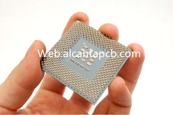
Um BGA/IC ultrafino substrato é um tipo de material de embalagem semicondutor significativamente mais fino que os substratos tradicionais, ao mesmo tempo que fornece o suporte mecânico e a conectividade elétrica necessários para circuitos integrados (ICS). Esses substratos são normalmente usados em Ball Grid Array (BGA) pacotes, que são amplamente utilizados na eletrônica moderna por suas capacidades de interconexão de alta densidade e formato compacto.
A espessura reduzida dos substratos BGA/IC ultrafinos é essencial para aplicações onde o espaço é escasso, como em dispositivos móveis, wearables, e outros eletrônicos compactos. Apesar de seu perfil fino, esses substratos devem manter excelente desempenho elétrico, estabilidade mecânica, e gerenciamento térmico para garantir a confiabilidade e a eficiência dos ICs que eles suportam.
Estrutura de substratos ultrafinos BGA/IC
A estrutura dos substratos BGA/IC ultrafinos é cuidadosamente projetada para equilibrar a necessidade de uma espessura reduzida com os requisitos de interconexões de alta densidade, integridade do sinal, e gerenciamento térmico. As principais características estruturais incluem:
O núcleo de um substrato BGA/IC ultrafino é normalmente feito de uma fina camada de resina epóxi reforçada ou materiais semelhantes que fornecem o suporte mecânico necessário enquanto minimizam a espessura. Este núcleo foi projetado para ser o mais fino possível sem comprometer a integridade estrutural do substrato.
Para atingir a densidade de circuito necessária, múltiplas camadas de acúmulo são adicionadas ao núcleo. Essas camadas são construídas com materiais dielétricos finos que oferecem excelente isolamento elétrico, mantendo um perfil discreto. As camadas de acúmulo permitem a criação de padrões de circuito complexos necessários para CIs de alto desempenho.
Os traços condutores em substratos BGAIC ultrafinos são normalmente feitos de cobre, que é depositado usando técnicas avançadas, como galvanoplastia ou pulverização catódica. Esses traços são padronizados com precisão para acomodar a fiação densa necessária para CIs modernos, garantindo perda mínima de sinal e desempenho de alta frequência.
As vias são essenciais para conectar diferentes camadas do substrato. Em substratos ultrafinos, microvias (vias muito pequenas) são frequentemente usados para manter o perfil fino enquanto fornecem conexões confiáveis entre camadas. Essas vias são criadas usando perfuração a laser ou outras técnicas de precisão.
As almofadas de contato em substratos BGAIC ultrafinos são finalizadas com materiais como ENIG (Ouro de imersão em níquel eletrolítico) ou OSP (Conservante Orgânico de Soldabilidade) para melhorar a soldabilidade e proteger contra a oxidação.
Materiais usados em substratos BGA/IC ultrafinos
Os materiais usados em substratos BGAIC ultrafinos são selecionados por sua capacidade de fornecer a energia elétrica necessária, térmico, e propriedades mecânicas, permitindo ao mesmo tempo uma espessura de substrato reduzida. Os principais materiais incluem:
Resinas epóxi de alto desempenho, muitas vezes reforçado com fibras de vidro, são usados como material central para substratos BGAIC ultrafinos. Estas resinas oferecem um equilíbrio de resistência mecânica, Estabilidade térmica, e isolamento elétrico, mesmo em camadas muito finas.
O cobre é o principal material utilizado para traços condutores devido à sua excelente condutividade elétrica. Em substratos ultrafinos, camadas de cobre são depositadas usando métodos que permitem padrões muito finos e controle sobre espessura, o que é crítico para manter a integridade do sinal.
Materiais dielétricos avançados com baixas constantes dielétricas e tangentes de baixa perda são usados nas camadas de construção. Esses materiais são essenciais para minimizar a atenuação do sinal e diafonia, que são considerações críticas em alta densidade, circuitos de alta frequência.
Acabamentos de superfície como ENIG e OSP são aplicados nas placas de contato para garantir juntas de solda confiáveis e proteger os vestígios de cobre da degradação ambiental. Esses acabamentos devem ser compatíveis com a estrutura ultrafina e não adicionar espessura significativa ao substrato.
O processo de fabricação de substratos BGA/IC ultrafinos
O processo de fabricação de substratos BGAIC ultrafinos envolve várias etapas precisas e controladas para garantir que o produto final atenda aos rigorosos requisitos da eletrônica moderna. As principais etapas incluem:
O processo começa com a seleção e preparação de materiais de alta qualidade, incluindo resinas epóxi, folhas de cobre, e filmes dielétricos. Esses materiais são escolhidos por sua capacidade de fornecer as propriedades necessárias em um formato fino.
A camada central é laminada com camadas dielétricas e de cobre para criar uma estrutura multicamadas. Este processo de laminação envolve um controle cuidadoso de pressão e temperatura para garantir que as camadas se unam corretamente sem adicionar espessura desnecessária.
Microvias são perfuradas no substrato usando tecnologia laser para conectar diferentes camadas do circuito. Essas vias são então revestidas com cobre para criar caminhos condutores. A precisão desta etapa é crucial para manter a integridade do substrato ultrafino.
As camadas de cobre são padronizadas usando fotolitografia ou técnicas similares para criar os traços de circuito desejados. Esta etapa deve ser executada com alta precisão para garantir que os circuitos estejam corretamente alinhados e que as larguras dos traços sejam consistentes com as especificações do projeto..
Uma máscara de solda é aplicada ao substrato para proteger os traços do circuito e evitar pontes de solda durante a montagem do pacote IC. A máscara de solda deve ser fina e aplicada com precisão para evitar adicionar volume ao substrato ultrafino.
As almofadas de contato são finalizadas com ENIG, OSP, ou outros revestimentos protetores para melhorar a soldabilidade e proteger os vestígios de cobre da oxidação. Esta etapa é cuidadosamente controlada para garantir que o acabamento superficial não comprometa o perfil fino do substrato.
Os substratos BGAIC ultrafinos finais passam por inspeção e testes rigorosos para garantir que atendam a todos os padrões de desempenho e confiabilidade. Isso inclui a verificação de defeitos, medição de espessura, e testar o desempenho elétrico.
Áreas de aplicação de substratos BGAIC ultrafinos
Substratos BGAIC ultrafinos são usados em uma variedade de aplicações de alto desempenho, aplicações eletrônicas com espaço limitado. As principais áreas de aplicação incluem:
Substratos BGAIC ultrafinos são ideais para smartphones, comprimidos, e outros dispositivos móveis onde o espaço é limitado, e integração de alta densidade é necessária. Esses substratos permitem a miniaturização de componentes sem sacrificar o desempenho.
Em dispositivos vestíveis, como smartwatches e rastreadores de fitness, substratos BGAIC ultrafinos fornecem a plataforma necessária para compactos, eletrônicos leves que oferecem funcionalidades avançadas como GPS, monitoramento de frequência cardíaca, e comunicação sem fio.
Substratos BGAIC ultrafinos são usados em aplicações de computação de alto desempenho, incluindo CPUs, GPU, e módulos de memória. A capacidade de suportar interconexões densas e gerenciamento térmico eficiente é fundamental nessas aplicações.
Substratos BGAIC ultrafinos são usados em equipamentos de telecomunicações, como estações base e switches de rede, onde o desempenho de alta frequência e os formatos compactos são essenciais para gerenciar a crescente demanda por transmissão de dados.
Vantagens dos substratos BGAIC ultrafinos
Os substratos BGAIC ultrafinos oferecem diversas vantagens que os tornam indispensáveis para aplicações eletrônicas modernas. Essas vantagens incluem:
A espessura reduzida dos substratos BGAIC ultrafinos permite o desenvolvimento de dispositivos eletrônicos menores e mais leves sem comprometer o desempenho. Isto é particularmente importante em aplicações como dispositivos móveis e wearables, onde o espaço é valioso.
Substratos ultrafinos permitem a criação de padrões de circuito de alta densidade, que são essenciais para suportar a funcionalidade complexa dos CIs modernos. Isso permite a integração de mais recursos em um espaço menor.
Apesar de seu perfil fino, substratos BGAIC ultrafinos mantêm excelente desempenho elétrico, com mínima perda de sinal e interferência. Isto é fundamental para aplicações de alta frequência e alta velocidade onde a integridade do sinal é fundamental.
Substratos BGAIC ultrafinos são projetados para dissipar o calor de forma eficaz, mesmo em dispositivos compactos. Isso ajuda a evitar o superaquecimento e garante a operação confiável dos componentes eletrônicos em ambientes exigentes.
Perguntas frequentes
Quais são os principais benefícios do uso de substratos BGAIC ultrafinos em dispositivos móveis?
Os substratos BGAIC ultrafinos são ideais para dispositivos móveis porque permitem uma miniaturização significativa, mantendo a integração de alta densidade e excelente desempenho elétrico. Isso permite que os fabricantes desenvolvam, isqueiro, e dispositivos mais poderosos.
Como os substratos BGAIC ultrafinos melhoram o gerenciamento térmico em eletrônicos compactos?
Substratos BGAIC ultrafinos são projetados com materiais e estruturas que melhoram a condutividade térmica, permitindo uma dissipação de calor eficiente mesmo em dispositivos compactos. Isso evita o superaquecimento e garante uma operação confiável, especialmente em aplicações de alta potência.
Os substratos BGAIC ultrafinos podem ser usados em aplicações de alta frequência?
Sim, substratos BGAIC ultrafinos são adequados para aplicações de alta frequência. Eles oferecem baixa perda dielétrica e alta integridade de sinal, tornando-os ideais para telecomunicações, RF, e circuitos de micro-ondas que exigem desempenho preciso e estável.
Quais indústrias se beneficiam mais com substratos BGAIC ultrafinos?
As indústrias que mais se beneficiam dos substratos BGAIC ultrafinos incluem a tecnologia móvel, eletrônicos vestíveis, computação de alto desempenho, e telecomunicações. Essas indústrias exigem equipamentos compactos, substratos de alto desempenho para suportar funcionalidades eletrônicas avançadas em aplicações com espaço limitado.