КОМПАНИЯ С ОГРАНИЧЕННОЙ ОТВЕТСТВЕННОСТЬЮ")
Производитель пакетных подложек ABF GL102R8HF. Ведущий ABF GL102R8HF. Подложки упаковки производитель, мы специализируемся на производстве высокопроизводительных подложек, предназначенных для передовых полупроводниковых приложений.. Наши продукты обеспечивают превосходную целостность сигнала, эффективное рассеяние тепла, и надежная механическая поддержка. Благодаря новейшим технологиям и строгому контролю качества., мы поставляем надежные решения, отвечающие меняющимся требованиям электронной промышленности.
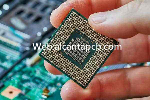
АБФ (Аджиномото наращивание фильма) Подложки корпусов GL102R8HF — это передовые материалы, используемые в современной полупроводниковой упаковке.. Эти субстраты играют решающую роль в поддержке соединений высокой плотности и повышенной производительности, необходимых для современных электронных устройств.. В этой статье рассматриваются свойства, структура, материалы, производственные процессы, приложения, преимущества, и часто задаваемые вопросы (Часто задаваемые вопросы) относится к подложкам корпуса ABF GL102R8HF.
Структура подложек корпуса ABF GL102R8HF
Структура подложек корпуса ABF GL102R8HF тщательно разработана с учетом жестких требований высокопроизводительных полупроводниковых приборов.:
ABF GL102R8HF — это высокоэффективная пленка из эпоксидной смолы, известная своей превосходной электроизоляцией., механическая сила, и термическая стабильность. Он служит основным диэлектрическим материалом в подложке..
Для электрических соединений используются несколько слоев меди.. Эти слои имеют точный рисунок для достижения высокой плотности межсоединений, необходимой для передовых полупроводниковых приложений..
Отведенная область на подложке, к которой полупроводниковый кристалл крепится с помощью клея или припоя.. Эта область должна обеспечивать отличную теплопроводность для рассеивания тепла, выделяемого микросхемой..
Определенные области на подложке, предназначенные для соединения проводов или соединения перевернутых кристаллов.. Эти подушечки обычно покрыты золотым покрытием, чтобы улучшить адгезию и предотвратить окисление..
Высокоэффективные диэлектрические материалы, например ABF GL102R8HF, разделить проводящие слои, обеспечение электрической изоляции и сохранение целостности сигнала.
Микроотверстия и сквозные отверстия используются для создания вертикальных соединений между различными слоями подложки., обеспечение высокой плотности маршрутизации и минимизация паразитной индуктивности и емкости.
Различная обработка поверхности, например ЭНИГ (Химическое никель, иммерсионное золото) или ОСП (Органические консерванты для пайки), применяются для защиты медных поверхностей и улучшения паяемости.
Материалы, используемые в подложках корпуса ABF GL102R8HF
Ключевые материалы, используемые в подложках корпуса ABF GL102R8HF, включают::
Высококачественная пленка из эпоксидной смолы с отличными электроизоляционными свойствами., высокая температура стеклования, и хорошая адгезия к меди, что делает его идеальным для межсоединений высокой плотности и передовых полупроводниковых приложений..
Медь высокой чистоты используется для проводящих дорожек из-за ее превосходной электропроводности и надежности..
Материалы с низкой диэлектрической проницаемостью и тангенсными потерями необходимы для поддержания высокой целостности сигнала и минимальных потерь сигнала..
Поверхностная обработка, такая как ENIG и OSP, используется для защиты медных дорожек от окисления и улучшения паяемости..
Процесс производства подложек корпуса ABF GL102R8HF
Процесс производства подложек корпусов ABF GL102R8HF включает в себя несколько точных этапов, обеспечивающих высокую производительность и надежность.:
Выбор подходящих базовых материалов и проводящих слоев в зависимости от требований к производительности..
Создание нескольких слоев проводящих и диэлектрических материалов с использованием пленки ABF GL102R8HF., формирование стабильной подложки уменьшенной толщины и улучшенных характеристик..
Прецизионное сверление, в том числе лазерное бурение, используется для создания микроотверстий и сквозных отверстий для вертикальных соединений.
Нанесение меди на подложку и внутренние переходные отверстия для создания надежных электрических соединений..
Использование фотолитографии и химического травления для определения схем и межсоединений..
Нанесение защитных покрытий на открытые медные поверхности для улучшения паяемости и защиты от окисления..
Крепление полупроводникового кристалла к подложке с использованием передовых технологий флип-чипа или проводного соединения., обеспечение минимальных потерь и искажений сигнала.
Герметизация матрицы для механической защиты и термической стабильности., с последующими строгими испытаниями на электрические характеристики, целостность сигнала, и соблюдение проектных требований.
Применение подложек корпуса ABF GL102R8HF
Подложки корпуса ABF GL102R8HF используются в широком спектре высокопроизводительных приложений., включая:
Смартфоны, таблетки, и другие портативные устройства, которым требуется компактный и высокопроизводительный корпус микросхемы..
Базовые станции, сетевое оборудование, и другие устройства связи, требующие высокочастотной передачи сигналов и надежного соединения..
Передовые системы помощи водителю (АДАС), информационно-развлекательные системы, и другие электронные компоненты в автомобилях.
Высокопроизводительные вычислительные системы и системы управления, используемые в автоматизации производства и технологических процессов..
Диагностическое и визуализирующее оборудование, требующее высокой надежности и точности..
Преимущества корпусных подложек ABF GL102R8HF
Подложки корпуса ABF GL102R8HF обладают рядом существенных преимуществ.:
Использование пленки ABF GL102R8HF позволяет создавать межсоединения высокой плотности., создание передовых полупроводниковых конструкций и повышение функциональности.
Низкая диэлектрическая проницаемость и малый тангенс потерь ABF GL102R8HF обеспечивают минимальные потери сигнала и высокую целостность сигнала., имеет решающее значение для высокоскоростных и высокочастотных приложений.
Высокая температура стеклования ABF GL102R8HF обеспечивает превосходную термическую стабильность., обеспечение надежной работы в условиях высоких температур.
Механические свойства ABF GL102R8HF способствуют общей долговечности и прочности основания., что делает его подходящим для требовательных приложений.
Подложки корпуса ABF GL102R8HF могут использоваться в широком спектре применений в различных отраслях промышленности., от бытовой электроники до автомобильной и медицинской техники.
Часто задаваемые вопросы
Что такое ABF GL102R8HF?, и почему он используется в подложках упаковки?
ABF GL102R8HF — это высокоэффективная пленка из эпоксидной смолы, известная своими превосходными электроизоляционными свойствами., высокая температура стеклования, и хорошая адгезия к меди. Он используется в подложках корпусов для обеспечения межсоединений высокой плотности., улучшить электрические характеристики, и повысить термическую стабильность.
Чем подложки корпуса ABF GL102R8HF отличаются от традиционных подложек?
В подложках корпуса ABF GL102R8HF используется высокоэффективная пленка, обеспечивающая более высокую плотность межсоединений., лучшие электрические характеристики, и улучшенная термическая стабильность по сравнению с традиционными подложками, в которых могут использоваться материалы с более низкими характеристиками..
Какие отрасли промышленности получают наибольшую выгоду от использования подложек корпусов ABF GL102R8HF??
Такие отрасли, как бытовая электроника, телекоммуникации, автомобильная электроника, промышленная автоматизация, и медицинские устройства значительно выигрывают от использования подложек корпусов ABF GL102R8HF благодаря их высокой плотности межсоединений., отличные электрические характеристики, и термическая стабильность.
Как тестируются подложки корпуса ABF GL102R8HF для обеспечения надежности?
Подложки корпусов ABF GL102R8HF проходят строгие испытания., включая электрические испытания целостности сигнала и производительности, термоциклирование, и тестирование надежности. Эти испытания гарантируют, что подложки соответствуют строгим стандартам производительности и долговечности, необходимым для высокопроизводительных приложений..