CO.,LTD")
ABF GZ41R2H Paketsubstrate Hersteller. Unser Unternehmen ist ein führender Hersteller von ABF GZ41R2H-Gehäusesubstraten, spezialisiert auf Hochleistungslösungen für fortschrittliche Elektronik. Mit modernster Technologie und strenger Qualitätskontrolle, Wir bieten zuverlässige und effiziente Substrate, die den anspruchsvollen Anforderungen der heutigen Halbleiterindustrie gerecht werden.
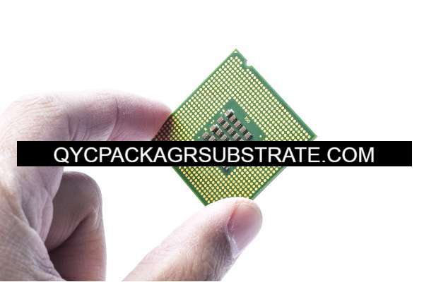
ABF GZ41R2H-Gehäusesubstrate stellen eine bahnbrechende Innovation auf dem Gebiet der Halbleiterverpackung dar. Diese Substrate spielen eine entscheidende Rolle bei der Leistungssteigerung, Zuverlässigkeit, und Miniaturisierung moderner elektronischer Geräte. Sie sind besonders wichtig bei Anwendungen mit hoher Dichte und hoher Leistung, wo Platzbeschränkungen und Wärmemanagement von entscheidender Bedeutung sind.
Was ist ein ABF GZ41R2H-Paketsubstrat??
ABF (Ajinomoto Aufbaufilm) Das GZ41R2H-Paketsubstrat ist eine Art Hochleistungssubstrat, das in Halbleitern verwendet wird Verpackung. Es ist darauf ausgelegt, die hochdichte Integration elektronischer Komponenten zu unterstützen und eine zuverlässige elektrische und thermische Leistung sicherzustellen.
Erweiterte Materialzusammensetzung: ABF-Substrate bestehen aus hochreinen Harzsystemen kombiniert mit Glasfaserverstärkungen, Bietet hervorragende mechanische Festigkeit und Stabilität.
Hochdichte Verbindung (HDI): Kann Fine-Pitch- und High-Density-Verbindungen unterstützen, Dies ermöglicht kompaktere und leistungsfähigere Halbleiterbauelemente.
Thermalmanagement: Entwickelt, um Wärme effektiv abzuleiten, Gewährleistung der Stabilität und Langlebigkeit elektronischer Komponenten.
Elektrische Leistung: Eine niedrige Dielektrizitätskonstante und ein niedriger Verlustfaktor sorgen für minimalen Signalverlust und eine schnelle Datenübertragung.
Zuverlässigkeit:Hohe thermische Stabilität und Beständigkeit gegen Feuchtigkeit und Chemikalien, Gewährleistung einer langfristigen Zuverlässigkeit unter verschiedenen Betriebsbedingungen.
Design-Referenzhandbuch für ABF GZ41R2H-Gehäusesubstrate
Bei der Entwicklung von ABF GZ41R2H-Gehäusesubstraten müssen mehrere wichtige Überlegungen berücksichtigt werden, um den Anforderungen moderner elektronischer Anwendungen gerecht zu werden.
Harzsysteme: Hochreine Harzsysteme bieten hervorragende elektrische Eigenschaften und thermische Stabilität.
Glasfaserverstärkungen: Verbessern Sie die mechanische Festigkeit und Dimensionsstabilität des Substrats.
Kupferfolien: Für Signal- und Leistungsschichten werden hochreine Kupferfolien verwendet, sorgt für eine hervorragende elektrische Leitfähigkeit.
Mehrschichtiger Aufbau:Unterstützt komplexe Designs mit mehreren Signal- und Leistungsschichten, Ermöglicht eine Integration mit hoher Dichte.
Kern- und Aufbauschichten:Kernschichten sorgen für strukturelle Integrität, während Aufbauschichten Fine-Pitch- und High-Density-Verbindungen ermöglichen.
Wärmeableitung:Effiziente Wärmeableitungstechniken sind für die Aufrechterhaltung der Leistung und Zuverlässigkeit unerlässlich.
Thermische Vias und Kühlkörper:Wird verwendet, um die Wärmeleitfähigkeit zu verbessern und den Wärmefluss innerhalb des Substrats zu steuern.
Kontrollierte Impedanz:Gewährleistung einer konsistenten Impedanz über alle Signalleitungen hinweg, um Signalreflexion und -verlust zu minimieren.
Niedrige Dielektrizitätskonstante:Reduziert die Signalverzögerung und verbessert die Hochgeschwindigkeits-Datenübertragung.
Fortgeschrittene Lithographie:Hochpräzise Lithographietechniken werden verwendet, um Verbindungen mit feinem Rastermaß und hoher Dichte zu definieren.
Galvanisieren und Ätzen:Präzise Beschichtungs- und Ätzprozesse gewährleisten die genaue Bildung von Leiterbahnen.
Welche Materialien werden in ABF GZ41R2H-Paketsubstraten verwendet??
ABF GZ41R2H-Gehäusesubstrate bestehen aus fortschrittlichen Materialien, die den strengen Anforderungen von Hochleistungs-Halbleitergehäusen gerecht werden.
Hochreine Harzsysteme:Bieten hervorragende elektrische Eigenschaften, thermische Stabilität, und mechanische Festigkeit.
Glasfaserverstärkungen: Verbessern Sie die Dimensionsstabilität und die mechanische Integrität.
Kupferfolien:Für Signal- und Leistungsschichten wird hochreines Kupfer verwendet, bietet hervorragende elektrische Leitfähigkeit und Zuverlässigkeit.
Vergoldung: Wird häufig zur Oberflächenveredelung verwendet, um langfristige Zuverlässigkeit und Oxidationsbeständigkeit zu gewährleisten.
Dielektrika mit niedrigem Dk-Wert:Um Signalverzögerungen und -verluste zu minimieren, werden Materialien mit niedrigen Dielektrizitätskonstanten verwendet, Gewährleistung einer schnellen Datenübertragung.
Thermische Schnittstellenmaterialien: Verbessern Sie die Wärmeableitung zwischen dem Substrat und anderen Komponenten.
Welche Größe haben ABF GZ41R2H-Paketsubstrate??
Die Größe der ABF GZ41R2H-Paketsubstrate kann je nach Anwendung und Designanforderungen variieren. Jedoch, Sie sind typischerweise so konzipiert, dass sie kompakt sind und in die Abmessungen moderner Halbleitergehäuse passen.
Benutzerdefinierte Abmessungen: Kann auf spezifische Anwendungen zugeschnitten werden, reicht von klein, komplizierte Designs für kompakte Geräte bis hin zu größeren Formaten für umfangreichere Systeme.
Panelgrößen:Die Fertigung beginnt häufig mit Standardplattengrößen, die dann auf die erforderlichen Maße zugeschnitten und bearbeitet werden.
Ultradünne Schichten: Die Gesamtdicke des Substrats kann nur wenige Millimeter betragen, wobei einzelne Schichten noch dünner sind.
Variable Dicke:Abhängig von der Anzahl der Schichten und den spezifischen Designanforderungen, Die Gesamtdicke kann angepasst werden, um Leistung und mechanische Stabilität in Einklang zu bringen.
Der Herstellungsprozess von ABF GZ41R2H-Paketsubstraten
Der Herstellungsprozess der ABF GZ41R2H-Gehäusesubstrate umfasst mehrere präzise Schritte, um sicherzustellen, dass das Endprodukt die strengen Anforderungen von Hochleistungsanwendungen erfüllt.
CAD-Design:Detaillierter Entwurf mittels computergestütztem Design (CAD) Software, unter Einbeziehung aller Komponenten, Lagen, und elektrische Pfade.
Simulation:Elektrisch, Thermal-, und mechanische Simulationen werden durchgeführt, um das Design hinsichtlich Leistung und Zuverlässigkeit zu optimieren.
Untergrundvorbereitung:Es werden hochwertige Untergründe vorbereitet, Für komplexe Designs sind oft mehrere Schichten erforderlich.
Laminierung: Die Schichten werden mithilfe fortschrittlicher Verfahren zusammenlaminiert, um Gleichmäßigkeit und Haftung zu gewährleisten.
Photolithographie:Mithilfe hochpräziser Fotolithographie werden die Schaltkreismuster auf dem Substrat definiert.
Radierung: Chemische oder Plasmaätzprozesse entfernen unerwünschtes Material, um die Leiterbahnen und Strukturen zu bilden.
Mikrobohren:Durch Laser- oder mechanisches Bohren entstehen Durchkontaktierungen und Löcher für Verbindungen zwischen den Schichten.
Überzug:Kupfer und andere Materialien werden auf die Durchkontaktierungen und Löcher plattiert, um eine elektrische Verbindung herzustellen.
Oberflächenbeschaffung: Aufbringen von Oberflächenveredelungen wie ENIG (Chemisches Nickel-Immersionsgold) oder HASL (Heißluft-Lotnivellierung) um das Kupfer zu schützen und die Lötbarkeit zu verbessern.
Montage:Die Montage der Komponenten erfolgt mittels Oberflächenmontagetechnik (SMT) oder Durchstecktechnik (Tht) nach Bedarf.
Elektrische Prüfung: Es werden strenge Tests durchgeführt, um sicherzustellen, dass alle Verbindungen intakt sind und das Substrat wie vorgesehen funktioniert.
Thermische Prüfung: Durch thermische Tests wird die Fähigkeit des Substrats überprüft, Wärme abzuleiten und die Leistung aufrechtzuerhalten.
Endkontrolle:Eine gründliche Prüfung stellt sicher, dass der Untergrund alle Designvorgaben und Qualitätsstandards erfüllt.
Der Anwendungsbereich von ABF GZ41R2H-Paketsubstraten
ABF GZ41R2H-Gehäusesubstrate werden in verschiedenen Hochleistungsanwendungen eingesetzt, bei denen Zuverlässigkeit gefragt ist, Effizienz, und Miniaturisierung sind unerlässlich.
Halbleiterverpackung: Wird in fortschrittlichen Halbleiterverpackungen verwendet, einschließlich Flip-Chip- und Wire-Bond-Pakete, um Leistung und Zuverlässigkeit zu verbessern.
Telekommunikation:Wird in Hochfrequenz-Kommunikationsgeräten eingesetzt, wie z. B. HF-Module, Antennen, und Basisstationen.
Rechenzentren: Integriert in Hochleistungsrechnersysteme und Rechenzentren für eine effiziente Datenverarbeitung und -speicherung.
Unterhaltungselektronik:Wird in Smartphones verwendet, Tabletten, und andere tragbare Geräte, bei denen kompakte Größe und hohe Leistung entscheidend sind.
Automobil:Eingesetzt in fortschrittlichen Fahrerassistenzsystemen (Adas), Infotainmentsysteme, und andere Automobilelektronik.
Was sind die Vorteile von ABF GZ41R2H-Paketsubstraten??
High-Density-Integration: Unterstützt Fine-Pitch- und High-Density-Verbindungen, Dies ermöglicht kompaktere und leistungsfähigere Halbleiterbauelemente.
Ausgezeichnetes Wärmemanagement: Effiziente Wärmeableitungstechniken sorgen für Stabilität und Langlebigkeit elektronischer Komponenten.
Überlegene elektrische Leistung: Eine niedrige Dielektrizitätskonstante und ein niedriger Verlustfaktor sorgen für minimalen Signalverlust und eine schnelle Datenübertragung.
Zuverlässigkeit: Hohe thermische Stabilität und Beständigkeit gegen Feuchtigkeit und Chemikalien, Gewährleistung einer langfristigen Zuverlässigkeit unter verschiedenen Betriebsbedingungen.
Vielseitigkeit:Kann mit benutzerdefinierten Abmessungen und Schichtaufbauten an spezifische Anwendungen angepasst werden, bietet Flexibilität im Design.
FAQ
Welche Materialien werden in ABF GZ41R2H-Paketsubstraten verwendet??
ABF GZ41R2H-Paketsubstrate verwenden fortschrittliche Materialien wie hochreine Harzsysteme, Glasfaserverstärkungen, und hochreine Kupferfolien.
Wie werden ABF GZ41R2H-Paketsubstrate hergestellt??
Der Herstellungsprozess umfasst CAD-Design, Materialvorbereitung, Photolithographie, Radierung, Bohren, Überzug, Abschluss, und strenge Tests und Qualitätskontrolle.
In welchen Branchen werden ABF GZ41R2H-Paketsubstrate am häufigsten verwendet??
Sie werden häufig in Halbleiterverpackungen verwendet, Telekommunikation, Rechenzentren, Unterhaltungselektronik, und Automobilanwendungen.
Was sind die Hauptvorteile der Verwendung von ABF GZ41R2H-Paketsubstraten??
Zu den Hauptvorteilen zählt die hohe Integrationsdichte, ausgezeichnetes Wärmemanagement, Überlegene elektrische Leistung, Zuverlässigkeit, und Vielseitigkeit.
Welche Größen sind für ABF GZ41R2H-Paketsubstrate erhältlich??
Diese Substrate können individuell auf bestimmte Abmessungen zugeschnitten werden, mit Dicken von nur wenigen Mils, je nach Anwendung und Leistungsanforderungen.