КОМПАНИЯ С ОГРАНИЧЕННОЙ ОТВЕТСТВЕННОСТЬЮ")
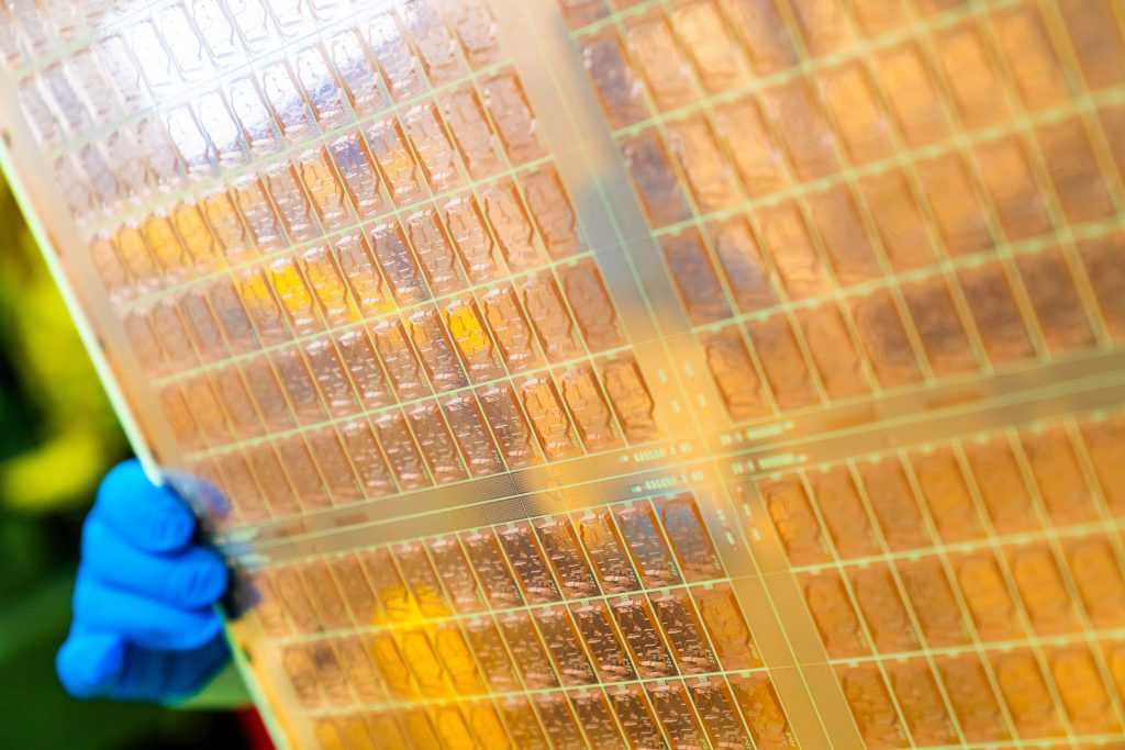
Передовой Полупроводниковые стеклянные подложки Производитель. Мы можем производить лучшие стеклянные подложки с самым высоким шагом с толщиной 100 мкм., лучший наименьший след и зазор — 9 мкм.
Усовершенствованные полупроводниковые стеклянные подложки являются важной частью современной электронной промышленности.. Это не только основные материалы для электронного оборудования., но также несут очень сложные схемы, обеспечение надежной поддержки для реализации различных передовых технологий. От смартфонов до медицинского оборудования, от космических кораблей до промышленной автоматизации, полупроводниковое стекло субстраты молча поддерживать бесчисленные инновации и производство. Благодаря своей превосходной производительности и надежности, они стали одним из незаменимых ключевых компонентов в современной электронной промышленности..
Что такое усовершенствованные полупроводниковые стеклянные подложки?
Усовершенствованные полупроводниковые стеклянные подложки являются одним из незаменимых базовых материалов в современном электронном производстве.. Они имеют сложную схемную структуру и играют жизненно важную роль в качестве платформы поддержки и подключения электронных устройств.. Полупроводниковые стеклянные подложки обычно изготавливаются из очень чистых стеклянных материалов, которые обладают превосходными электроизоляционными свойствами и механической прочностью и могут работать в экстремальных условиях., включая среду с высокой температурой и высоким давлением.
Процесс изготовления полупроводниковых стеклянных подложек очень сложен и требует строгого контроля и обработки.. Первый, высококачественное стекольное сырье отбирается, тщательно обрабатывается и обрабатывается с помощью специальных процессов и технологий, чтобы обеспечить чистоту и однородность материала.. Затем стеклянный материал разрезается на подложки необходимого размера и формы., часто используется современное режущее и шлифовальное оборудование для обеспечения плоскостности и точности основы.. Следующий, поверхность поверхности обработана, включая такие этапы, как очистка, покрытие, и фотолитография, при подготовке к изготовлению и сборке схем.
Полупроводниковые стеклянные подложки обладают множеством превосходных свойств., что делает их одним из предпочтительных материалов для производства электроники.. Первый, они обладают отличными электроизоляционными свойствами и могут эффективно изолировать сигналы и токи между цепями., снижение помех и потерь. Во-вторых, полупроводниковая стеклянная подложка обладает хорошей механической прочностью и стабильностью., выдерживает высокое давление и высокую температуру окружающей среды, и обеспечивает надежную работу электронного оборудования. Кроме того, Процесс производства полупроводниковых стеклянных подложек является зрелым, себестоимость производства относительно низкая, и он подходит для крупномасштабного производства и применения.
Полупроводниковые стеклянные подложки широко используются в электронном производстве., включая смартфоны, таблетки, дисплеи, датчики и другие электронные устройства. Они используются не только для подключения и поддержки электронных компонентов., но также несут сложные схемные структуры и функциональные модули., обеспечивая важную гарантию высокой производительности и высокой надежности современного электронного оборудования.
В итоге, полупроводниковые стеклянные подложки, как важная часть современной электронной промышленности, имеют отличные характеристики и широкие перспективы применения. Благодаря постоянному развитию и инновациям науки и техники, Считается, что полупроводниковые стеклянные подложки будут играть более важную роль в будущей электронной промышленности., подталкивая всю отрасль к более интеллектуальному, эффективное и устойчивое направление развития.
Справочное руководство по проектированию усовершенствованных полупроводниковых стеклянных подложек.
Проектирование полупроводниковых стеклянных подложек — сложная и ответственная задача, требующая комплексного учета многих факторов.. Прежде всего, Компоновка схемы является важной частью конструкции. Инженерам необходимо точно спланировать расположение и соединение компонентов схемы, чтобы обеспечить эффективную и стабильную передачу сигнала.. Оптимизация компоновки может снизить риск помех сигнала и перекрестных помех, а также улучшить общую производительность..
Во-вторых, передача сигнала является еще одним важным фактором в процессе проектирования.. Полупроводниковые стеклянные подложки часто используются в высокочастотных системах., приложения для высокоскоростной передачи сигналов, поэтому конструкция линий передачи сигнала должна быть тщательно спроектирована, чтобы обеспечить качество и стабильность сигнала.. Инженерам необходимо учитывать длину сигнальной линии, ширина, согласование импеданса и другие параметры для минимизации затухания и искажений сигнала.
Кроме того, Управление температурным режимом также является частью, которую нельзя игнорировать в процессе проектирования.. Полупроводниковые приборы во время работы выделяют большое количество тепла.. Если тепло не может быть эффективно рассеяно, производительность и стабильность устройства будут затронуты. Поэтому, при проектировании полупроводниковых стеклянных подложек, инженерам необходимо разумно расположить компоненты рассеивания тепла и продумать конструкцию вентиляции и рассеивания тепла зоны нагрева, чтобы гарантировать правильную работу оборудования в условиях высоких температур..
В итоге, проектирование полупроводниковых стеклянных подложек требует всестороннего рассмотрения схемы схемы., передача сигнала, и термоменеджмент. Использование справочного руководства, инженеры могут систематически оптимизировать конструкции для повышения производительности и надежности., обеспечение оптимальной работы полупроводниковых стеклянных подложек в различных приложениях..
Какой материал используется в передовых полупроводниковых стеклянных подложках?
Материал полупроводниковой стеклянной подложки является ключевым компонентом ее конструкции и характеристик.. Обычно, эти подложки изготовлены из стеклянных материалов высокой чистоты, которые специально обработаны для удовлетворения строгих требований полупроводниковой промышленности к химической стабильности и теплопроводности..
В процессе производства полупроводниковых стеклянных подложек, сначала необходимо выбрать сырье с соответствующими физическими и химическими свойствами.. Это сырье смешивается и тщательно обрабатывается, чтобы гарантировать, что конечная стеклянная подложка имеет однородный химический состав и микроструктуру.. Этот стеклянный материал высокой чистоты имеет чрезвычайно низкое содержание примесей и обеспечивает отличные электроизоляционные свойства., эффективно предотвращает утечку тока и помехи в цепях.
Помимо превосходной химической стабильности, Полупроводниковые стеклянные подложки также должны иметь хорошие свойства теплопроводности.. Во время работы электронного оборудования, будет выделяться большое количество тепла. Если тепло не может быть эффективно рассеяно, это может привести к перегреву и снижению производительности компонентов схемы.. Поэтому, материал полупроводниковой стеклянной подложки должен иметь хорошую теплопроводность, чтобы эффективно отводить тепло в окружающую среду и поддерживать стабильную работу схемы..
После точной обработки и оптимизированного дизайна, материал полупроводниковой стеклянной подложки обеспечивает стабильность и надежность схемы. Их однородная структура и плоскостность поверхности обеспечивают правильное соединение и надежность электронных компонентов.. Кроме того, эти материалы обладают превосходной коррозионной стойкостью и механической прочностью., позволяя им сохранять стабильность в суровых условиях окружающей среды.
Общий, Полупроводниковые стеклянные подложки являются жизненно важной частью современной электронной промышленности.. Они не только несут в себе сложные схемы, но также обеспечить производительность и надежность электронного оборудования, обеспечение стабильной базовой поддержки различных приложений.
Каковы размеры усовершенствованных полупроводниковых стеклянных подложек??
Полупроводниковые стеклянные подложки различаются по размеру в зависимости от применения., позволяя им адаптироваться к потребностям множества различных устройств. Полупроводниковые стеклянные подложки доступны в широком диапазоне размеров., от подложек размером с микрочип до подложек для дисплеев большой площади, обеспечение гибкости и возможности настройки при проектировании различных электронных устройств.
Что касается микроразмера, Полупроводниковые стеклянные подложки часто проектируются как подложки размером с кристаллы для размещения микросхем и интегральных схем.. Эти подложки обычно очень малы по размеру, чтобы соответствовать размеру микрочипов и потребностям многофункциональных конструкций.. Микроподложки требуют чрезвычайно высокой точности размеров и стабильности для обеспечения производительности и надежности схемы..
С другой стороны, Подложки для экранов дисплеев большой площади — еще одна важная область применения полупроводниковых стеклянных подложек.. Эти подложки обычно используются при производстве жидкокристаллических дисплеев. (ЖК-дисплеи), органические светодиоды (OLED-дисплеи) и другие технологии плоских дисплеев. Подложки для дисплеев могут быть очень большими по размеру., настраивается под размер и разрешение конкретного дисплея. Эти подложки должны иметь превосходную плоскостность и оптические свойства, чтобы обеспечить качество и стабильность изображения на дисплее..
И не только это, Полупроводниковые стеклянные подложки также играют важную роль во многих других приложениях., такие как датчики, оптические устройства, и медицинское оборудование. В этих областях, размеры подложек могут варьироваться от микро до больших, настраивается в соответствии с требованиями конкретного применения.
В общем, Полупроводниковые стеклянные подложки доступны в гибких размерах для удовлетворения потребностей различных устройств и приложений.. Будь то подложка уровня микрочипа или подложка дисплея большой площади., отражена важность полупроводниковых стеклянных подложек как незаменимого ключевого компонента в современной электронной промышленности..
Процесс изготовления усовершенствованных полупроводниковых стеклянных подложек.
Процесс производства полупроводниковых стеклянных подложек — это очень сложный процесс, включающий множество сложных этапов, призванных обеспечить качество и стабильность схемы.. Эти шаги подробно описаны ниже..
Первым делом идет подготовка стеклянной подложки.. Этот шаг имеет решающее значение, поскольку качество субстрата напрямую влияет на успех последующих процессов.. В процессе подготовки, необходимо выбрать стеклянные материалы высокой чистоты и получить плоскую поверхность и соответствующую толщину посредством точных процессов резки и полировки.. Качество поверхности стеклянной подложки имеет решающее значение для последующих процессов фотолитографии и травления., поэтому необходимо обеспечить чистоту и плоскостность поверхности..
Далее идет процесс фотолитографии.. На этом этапе, светочувствительный клей нанесен на поверхность стеклянной подложки, и фотолитографическая машина используется для проецирования разработанного рисунка на светочувствительный клей.. Благодаря ультрафиолетовому облучению и химической обработке., необходимая графика может быть сформирована на светочувствительном клее. Точность и стабильность процесса фотолитографии имеют решающее значение для точности и производительности схемы., поэтому требуется прецизионное оборудование и строгий контроль процесса..
Затем идет процесс травления.. На этом этапе, раствор химического травления используется для удаления участков, не покрытых фотолитографией, с поверхности стеклянной подложки для формирования желаемой структуры схемы.. Точность и избирательность процесса травления имеют решающее значение для качества и стабильности схемы., поэтому требуется точный контроль процесса и соответствующие рецептуры травильного раствора..
Последний этап – процесс металлизации.. На этом этапе, металлические провода или соединители образуются на поверхности стеклянной подложки в результате испарения или других процессов осаждения металла.. Точность и однородность процесса металлизации имеют решающее значение для проводимости и стабильности цепи., поэтому требуется прецизионное оборудование для осаждения металла и строгий контроль процесса..
В общем, Процесс производства полупроводниковых стеклянных подложек включает в себя несколько сложных этапов и требует очень сложного оборудования и технологий для обеспечения качества и стабильности схемы.. Только при строгом контроле процесса можно добиться высокого качества, производство высокопроизводительных полупроводниковых стеклянных подложек для удовлетворения потребностей современной электронной промышленности..
Область применения современных полупроводниковых стеклянных подложек.
Как важная часть электронной промышленности, Полупроводниковые стеклянные подложки широко используются в различных электронных устройствах., и области их применения разнообразны, включая, помимо прочего, смартфоны, таблетки, дисплеи, и датчики. В этих устройствах, полупроводниковые стеклянные подложки играют ключевую роль, а их превосходная производительность и стабильность стали неотъемлемой частью современной электронной промышленности..
Смартфоны являются типичным примером применения полупроводниковых стеклянных подложек.. В смартфонах, В качестве основного материала материнской платы используются полупроводниковые стеклянные подложки., перенос основных схем и компонентов чипа телефона. В то же время, они также используются в модулях экранных дисплеев для защиты и поддержки панелей дисплея.. Его превосходные электрические характеристики и механическая прочность обеспечивают стабильную работу телефона и его способность выдерживать удары и давление при ежедневном использовании..
Планшетные компьютеры являются еще одним примером применения полупроводниковых стеклянных подложек.. В конструкции планшетных компьютеров, Полупроводниковые стеклянные подложки широко используются в ключевых компонентах, таких как материнские платы., дисплеи, и сенсорные панели. Высокая степень интеграции и отличные электрические характеристики обеспечивают стабильность и производительность планшета.. В то же время, полупроводниковая стеклянная подложка также может стать более тонкой и легкой., сделать планшетные компьютеры более портативными и простыми в использовании.
Область отображения также является одним из важных сценариев применения полупроводниковых стеклянных подложек.. В различных технологиях отображения, таких как жидкокристаллические дисплеи. (ЖК-дисплеи), органические светодиоды (OLED-дисплеи) и микродисплеи, Подложки из полупроводникового стекла играют роль поддержки и защиты панелей.. Его высокая прозрачность и однородность обеспечивают четкие и стабильные эффекты отображения., позволяя пользователям получить лучший визуальный опыт.
Кроме того, Полупроводниковые стеклянные подложки также широко используются в области датчиков.. В различных сенсорных устройствах, такие как камеры, считыватели отпечатков пальцев, и датчики окружающей среды, полупроводниковые стеклянные подложки используются в качестве носителей и упаковочных материалов для защиты сенсорных чипов и обеспечения стабильной рабочей среды.. Его превосходная химическая стабильность и устойчивость к высоким температурам позволяют датчику надежно работать в различных суровых условиях и широко используются в промышленном управлении., автомобильная электроника, умный дом и другие области.
В общем, Полупроводниковые стеклянные подложки широко используются в различных электронных устройствах благодаря своим превосходным характеристикам и стабильности.. Как неотъемлемая часть современной электронной промышленности., они обеспечивают прочную основу для высокой производительности и надежной работы различных устройств..
Каковы преимущества усовершенствованных полупроводниковых стеклянных подложек??
Преимущество подложек из полупроводникового стекла заключается в их выдающихся характеристиках по сравнению с традиционными подложками во многих аспектах.. Первый, полупроводниковые стеклянные подложки имеют более высокую степень интеграции. В процессе производства используются передовые технологии микрообработки., позволяя разместить больше компонентов схемы в относительно небольшом пространстве. Это позволяет реализовать более сложные электронные функции на подложке того же размера., тем самым улучшая производительность и функциональность устройства.
Во-вторых, Полупроводниковые стеклянные подложки имеют лучшие электрические свойства.. Потому что само стекло обладает отличными изоляционными свойствами., это уменьшает помехи и перекрестные помехи между цепями. Это означает более высокую скорость передачи сигнала и более стабильное качество сигнала., тем самым улучшая скорость отклика устройства и эффективность передачи данных.
Кроме того, Полупроводниковые стеклянные подложки обладают лучшими возможностями терморегулирования.. Стеклянный материал обладает хорошей теплопроводностью и может эффективно отводить тепло, выделяемое контуром, в окружающую среду.. Это помогает предотвратить повреждение схемы из-за перегрева и повышает стабильность и надежность устройства..
Самое главное, полупроводниковые стеклянные подложки обладают более высокой надежностью и стабильностью.. Производственный процесс строго контролируется, а материалы тщательно отбираются., обеспечивая длительный срок службы и меньший процент отказов. Это делает подложку из полупроводникового стекла подходящей для различных суровых условий эксплуатации., например, высокая температура, высокая влажность, высокое давление, и т. д., сохраняя при этом стабильную производительность, тем самым обеспечивая непрерывную работу оборудования.
Подводить итоги, Полупроводниковые стеклянные подложки имеют отличные характеристики с точки зрения интеграции., Электрические характеристики, возможности и надежность управления температурным режимом, и являются незаменимым и важным компонентом современного электронного оборудования.. Их превосходные характеристики позволяют использовать их в различных областях., предоставление мощной поддержки и стимула для развития электронной промышленности.
Часто задаваемые вопросы
Подходят ли полупроводниковые стеклянные подложки для работы в условиях высоких температур??
Да, Подложки из полупроводникового стекла обычно изготавливаются из жаропрочного стекла и обладают превосходной устойчивостью к высоким температурам.. Они могут стабильно работать в условиях высоких температур и подходят для различных промышленных и автомобильных применений..
Какова цена полупроводниковой стеклянной подложки?
Цены на полупроводниковые стеклянные подложки варьируются в зависимости от материала., размер и процесс изготовления. Вообще говоря, их цена относительно высока, но их производительность и стабильность могут обеспечить более высокую стоимость по сравнению с другими высокопроизводительными подложками..
Толщина полупроводниковой стеклянной подложки?
Толщина подложек полупроводникового стекла обычно составляет от десятков микрон до нескольких миллиметров.. Выбор толщины зависит от конкретных требований применения и обычно определяется на основе таких факторов, как сложность схемы., требования к терморегулированию, и механическая прочность.
Подвержены ли полупроводниковые стеклянные подложки механическим повреждениям??
Хотя полупроводниковые стеклянные подложки обладают превосходной механической прочностью., они все равно могут получить механические повреждения в экстремальных обстоятельствах. Поэтому, Во время проектирования и использования необходимо принять соответствующие защитные меры для обеспечения его стабильности и надежности..