CO.,LTD")
KI-Beschleunigermodul Leiterplatte Hersteller. Ein Hersteller von Leiterplatten für KI-Beschleunigermodule ist auf die Herstellung von Hochleistungsleiterplatten spezialisiert, die speziell für KI-Beschleunigermodule entwickelt wurden. Diese Leiterplatten wurden entwickelt, um die hohen Verarbeitungsanforderungen von Anwendungen der künstlichen Intelligenz zu unterstützen, Gewährleistung einer effizienten Datenübertragung und eines zuverlässigen Betriebs. Der Hersteller setzt modernste Technologie und Materialien ein, um Robustheit zu schaffen, hohe Geschwindigkeit Schaltkreise, die komplexe Algorithmen und umfangreiche Berechnungen verarbeiten können. Mit Fokus auf Präzision und Qualität, Sie stellen wesentliche Komponenten bereit, die die nächste Generation von KI-Technologien vorantreiben, sowohl Leistung als auch Effizienz steigern.
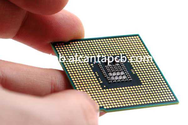
KI-Beschleunigermodul-Leiterplatten sind spezielle Leiterplatten, die zur Aufnahme und Unterstützung von KI-Beschleunigermodulen entwickelt wurden, Hierbei handelt es sich um Hardwarekomponenten, die für die Leistungssteigerung künstlicher Intelligenz optimiert sind (KI) und maschinelles Lernen (ML) Anwendungen. Diese Leiterplatten sind für die Bewältigung der hohen Verarbeitungsanforderungen von entscheidender Bedeutung, effiziente Datenübertragung, und Leistungsanforderungen von KI-Beschleunigern. Dieser Artikel befasst sich mit dem Konzept, Struktur, Materialien, Herstellungsprozess, Anwendungen, und Vorteile von AI Accelerator Module PCBs.
Was ist eine KI-Beschleunigermodul-Leiterplatte??
Eine KI-Beschleunigermodul-Leiterplatte ist eine Art Leiterplatte, die für die Integration von KI-Beschleunigermodulen entwickelt wurde, Dabei handelt es sich um spezielle Chips oder Prozessoren, die zur Beschleunigung von KI- und ML-Aufgaben entwickelt wurden. Diese Leiterplatten erleichtern den reibungslosen Betrieb von KI-Beschleunigern, indem sie die notwendigen elektrischen Verbindungen bereitstellen, Energieverwaltung, und thermische Lösungen. KI-Beschleunigermodul-Leiterplatten sind für Anwendungen, die eine hohe Rechenleistung und -geschwindigkeit erfordern, von entscheidender Bedeutung, wie Rechenzentren, autonome Systeme, und fortschrittliche Robotik.
Struktur der Leiterplatten des KI-Beschleunigermoduls
Die Struktur der Leiterplatten des KI-Beschleunigermoduls wurde sorgfältig entwickelt, um eine optimale Leistung und Zuverlässigkeit der KI-Beschleuniger zu gewährleisten. Zu den wichtigsten Strukturelementen gehören::
Das Kernmaterial besteht typischerweise aus Hochleistungssubstraten wie FR-4, Polyimid, oder Metallkern-Leiterplatten (MCPCBs). Diese Materialien bieten eine hervorragende mechanische Festigkeit, thermische Stabilität, und elektrische Eigenschaften.
Auf das Kernmaterial werden mehrere Kupferschichten laminiert, um die elektrischen Leiterbahnen zu bilden. Diese Schichten sind präzise strukturiert, um Verbindungen für KI-Beschleuniger und andere Komponenten herzustellen, Gewährleistung einer effizienten Daten- und Energieübertragung.
Zur Isolierung der leitenden Schichten werden fortschrittliche dielektrische Materialien verwendet, Gewährleistung minimaler Signalverluste und Störungen. Diese Materialien werden aufgrund ihrer niedrigen Dielektrizitätskonstante und hohen thermischen Leistung ausgewählt.
Durchkontaktierungen, einschließlich Durchkontaktierungen, Blind Vias, und Microvias, werden verwendet, um vertikale elektrische Verbindungen zwischen verschiedenen Schichten der Leiterplatte herzustellen. Diese Strukturen sind für die Erzielung hochdichter Verbindungen und komplexes Routing, die für KI-Beschleunigermodule erforderlich sind, von entscheidender Bedeutung.
AI-Beschleunigermodul-Leiterplatten verfügen über Wärmemanagementfunktionen wie Kühlkörper, thermische Durchkontaktierungen, und Kupferebenen zur Ableitung der von Hochleistungskomponenten erzeugten Wärme. Ein effizientes Wärmemanagement ist entscheidend für die Aufrechterhaltung der Leistung und Langlebigkeit von KI-Beschleunigern.
Das PCB-Design umfasst robuste Stromversorgungsnetzwerke, um eine stabile und effiziente Stromversorgung für KI-Beschleuniger und andere kritische Komponenten sicherzustellen. Dies erfordert eine sorgfältige Konstruktion der Antriebsflugzeuge, Entkopplungskondensatoren, und Spannungsregler.
Die Oberfläche der Leiterplatte ist mit Lacken wie ENIG beschichtet (Chemisches Nickel-Immersionsgold) oder OSP (Organisches Lötbarkeitskonservierungsmittel) um die Lötbarkeit zu verbessern und die Leiterbahnen vor Oxidation und Korrosion zu schützen.
Auf die Leiterplatte wird eine Schutzschicht aus Lötstopplack aufgetragen, um Lötbrücken zu verhindern und die Schaltung vor Umweltschäden zu schützen.
Materialien, die in Leiterplatten von KI-Beschleunigermodulen verwendet werden
Die Wahl der Materialien in AI-Beschleunigermodul-Leiterplatten ist entscheidend für deren Leistung und Zuverlässigkeit. Zu den gängigen Materialien gehören::
Hochleistungsmaterialien wie FR-4, Polyimid, und MCPCBs werden verwendet, um die notwendige mechanische Festigkeit bereitzustellen, thermische Stabilität, und elektrischen Eigenschaften, die für Hochleistungsanwendungen erforderlich sind.
Kupfer ist aufgrund seiner hohen elektrischen Leitfähigkeit und thermischen Leistung das primäre leitfähige Material, das in Leiterplatten von KI-Beschleunigermodulen verwendet wird. In einigen Fällen, Andere Metalle wie Gold oder Silber können für bestimmte Anwendungen verwendet werden, die eine höhere Leitfähigkeit oder Korrosionsbeständigkeit erfordern.
Fortschrittliche dielektrische Materialien wie Epoxidharz, Polyimid, und PTFE (Polytetrafluorethylen) dienen der Isolierung der leitenden Schichten. Diese Materialien bieten eine hervorragende elektrische Isolierung, thermische Stabilität, und chemische Beständigkeit.
Materialien mit hoher Wärmeleitfähigkeit, wie Aluminium oder Kupfer, werden für Kühlkörper und thermische Durchkontaktierungen verwendet, um die Wärme von Hochleistungskomponenten effizient abzuleiten.
ZUSTIMMEN, OSP, und Tauchzinn sind gängige Oberflächenveredelungen, die die Lötbarkeit verbessern und die Leiterplatte vor Oxidation und Korrosion schützen.
Lötmasken auf Epoxidharzbasis werden üblicherweise verwendet, um die Schaltkreise zu schützen und Lötbrücken während des Montageprozesses zu verhindern.
Der Herstellungsprozess von Leiterplatten für KI-Beschleunigermodule
Der Herstellungsprozess von AI Accelerator Module-Leiterplatten umfasst mehrere präzise und kontrollierte Schritte, um eine hohe Qualität und Leistung sicherzustellen. Zu den wichtigsten Schritten gehören::
In der Entwurfsphase werden detaillierte Schaltpläne und Layouts mithilfe computergestützter Konstruktion erstellt (CAD) Software. Das Layout umfasst die Anordnung der Leiterbahnen, Durchkontaktierungen, Wärmemanagementfunktionen, und andere Komponenten, die für die Funktionalität des KI-Beschleunigers erforderlich sind.
Hochwertige Rohstoffe, einschließlich Kernmaterialien, Kupferfolien, und dielektrische Materialien, werden vorbereitet und geprüft, um sicherzustellen, dass sie den erforderlichen Spezifikationen entsprechen.
Das Kernmaterial und die Kupferfolien werden durch Hitze und Druck miteinander laminiert, um eine einheitliche mehrschichtige Struktur zu bilden. Dieser Schritt erfordert eine präzise Ausrichtung und Kontrolle, um sicherzustellen, dass die Schichten richtig verbunden sind.
Vias und Microvias werden in die Leiterplatte gebohrt, um vertikale elektrische Verbindungen herzustellen. Diese Löcher werden dann mit Kupfer plattiert, um leitende Pfade herzustellen.
Die Schaltungsmuster werden mithilfe fotolithografischer Verfahren erstellt. Dabei wird ein lichtempfindlicher Film aufgebracht (Fotolack) zur Kupferoberfläche, indem man es ultraviolettem Licht aussetzt (UV) Licht durch eine Maske, und Entwickeln der freigelegten Bereiche, um die gewünschten Schaltkreismuster freizulegen. Anschließend wird die Leiterplatte geätzt, um das unerwünschte Kupfer zu entfernen, die Schaltkreisspuren hinterlassen.
Zur Isolierung der leitenden Schichten werden dielektrische Schichten aufgebracht. Bei diesem Schritt wird die Leiterplatte mit einem dielektrischen Material beschichtet und ausgehärtet, um eine feste Schicht zu bilden.
Kühlkörper, thermische Durchkontaktierungen, und Kupferflächen sind in die Leiterplatte integriert, um die Wärmeableitung zu steuern. Dieser Schritt ist entscheidend für den zuverlässigen Betrieb von Hochleistungs-KI-Beschleunigern.
Oberflächenveredelungen wie ENIG, OSP, Um die Lötbarkeit zu verbessern und vor Oxidation zu schützen, werden auf die Kontaktpads Tauchzinn oder Tauchzinn aufgetragen. Diese Oberflächen werden durch Galvanisieren oder Eintauchen aufgetragen.
Auf die Leiterplatte wird eine Schutzschicht aus Lötstopplack aufgetragen, um Lötbrücken zu verhindern und die Schaltung vor Umweltschäden zu schützen. Die Lötstoppmaske wird typischerweise mit Siebdruck- oder Fotolithografietechniken aufgetragen.
Die fertigen Leiterplatten werden strengen Inspektionen und Tests unterzogen, um sicherzustellen, dass sie alle Leistungs- und Zuverlässigkeitsstandards erfüllen. Elektrische Prüfung, Sichtprüfung, und automatisierte optische Inspektion (AOI) dienen der Feststellung etwaiger Mängel oder Unregelmäßigkeiten.
Anwendungsbereiche von AI-Beschleunigermodul-Leiterplatten
KI-Beschleunigermodul-Leiterplatten werden in einer Vielzahl elektronischer Anwendungen in verschiedenen Branchen eingesetzt. Zu den wichtigsten Anwendungsbereichen gehören:
Leiterplatten für KI-Beschleunigermodule sind in Rechenzentren für die Beschleunigung von KI- und ML-Arbeitslasten unerlässlich. Sie unterstützen Hochleistungsrechnen und effiziente Datenverarbeitung, Dadurch können Rechenzentren große Datenmengen und komplexe Berechnungen verarbeiten.
In autonomen Fahrzeugen, AI-Beschleunigermodul-Leiterplatten werden zur Verarbeitung von Sensordaten verwendet, Entscheidungen in Echtzeit treffen, und Steuerung von Fahrzeugsystemen. Ihre hohe Leistungsfähigkeit und Zuverlässigkeit sind entscheidend für den sicheren und effizienten Betrieb autonomer Fahrzeuge.
KI-Beschleunigermodul-Leiterplatten werden in der fortgeschrittenen Robotik für Aufgaben wie die Objekterkennung verwendet, Wegplanung, und Entscheidungsfindung in Echtzeit. Sie ermöglichen es Robotern, komplexe Aufgaben mit hoher Genauigkeit und Effizienz auszuführen.
In der Gesundheitsbranche, AI-Beschleunigermodul-Leiterplatten werden in der medizinischen Bildgebung eingesetzt, Diagnostik, und Patientenüberwachungssysteme. Sie unterstützen fortschrittliche KI-Algorithmen, die die Genauigkeit und Effizienz medizinischer Technologien verbessern.
AI-Beschleunigermodul-Leiterplatten werden in Telekommunikationsgeräten verwendet, um die Signalverarbeitung zu verbessern, Netzwerkmanagement, und Datenübertragung. Sie ermöglichen eine effiziente und zuverlässige Kommunikation in Hochgeschwindigkeitsnetzen.
Vorteile von AI-Beschleunigermodul-Leiterplatten
AI-Beschleunigermodul-Leiterplatten bieten mehrere Vorteile, die sie für moderne elektronische Anwendungen unverzichtbar machen. Zu diesen Vorteilen gehören:
AI-Beschleunigermodul-Leiterplatten sind für die Unterstützung von Hochleistungsrechnen konzipiert, Ermöglicht eine effiziente Datenverarbeitung und -berechnung für KI- und ML-Workloads.
Die Integration von Thermomanagementfunktionen sorgt für eine effiziente Wärmeableitung, Aufrechterhaltung der Leistung und Langlebigkeit von Hochleistungs-KI-Beschleunigern.
Der strenge Herstellungsprozess und die hochwertigen Materialien stellen sicher, dass die Leiterplatten des KI-Beschleunigermoduls strenge Leistungs- und Zuverlässigkeitsstandards erfüllen, Reduzierung des Risikos von Ausfällen in realen Anwendungen.
AI-Beschleunigermodul-Leiterplatten können einfach skaliert werden, um verschiedene Leistungsniveaus zu unterstützen, Dadurch sind sie an verschiedene Anwendungsanforderungen und zukünftige Weiterentwicklungen anpassbar.
Die Verwendung standardisierter Herstellungsprozesse und Materialien in AI Accelerator Module PCBs ermöglicht eine kostengünstige Produktion, Dies macht sie zu einer wirtschaftlichen Wahl für hochvolumige elektronische Anwendungen.
FAQ
Welche Materialien werden üblicherweise im Kern von AI-Beschleunigermodul-Leiterplatten verwendet??
Zu den gängigen Materialien, die im Kern von KI-Beschleunigermodul-Leiterplatten verwendet werden, gehört FR-4, Polyimid, und Metallkern-Leiterplatten (MCPCBs). Diese Materialien sorgen für die nötige mechanische Festigkeit, thermische Stabilität, und elektrischen Eigenschaften, die für Hochleistungsanwendungen erforderlich sind.
Wie verbessern AI Accelerator Module-Leiterplatten die Leistung von Rechenzentren??
AI Accelerator Module-Leiterplatten verbessern die Leistung von Rechenzentren, indem sie eine effiziente Datenverarbeitung und Berechnung für KI- und ML-Workloads ermöglichen. Sie unterstützen Hochleistungsrechnen und sorgen für eine stabile und effiziente Stromversorgung, Dadurch können Rechenzentren große Datenmengen und komplexe Berechnungen verarbeiten.
Können KI-Beschleunigermodul-Leiterplatten in autonomen Fahrzeugen verwendet werden??
Ja, KI-Beschleunigermodul-Leiterplatten eignen sich hervorragend für autonome Fahrzeuge. Sie dienen der Verarbeitung von Sensordaten, Entscheidungen in Echtzeit treffen, und Steuerung von Fahrzeugsystemen.
Was sind die Hauptvorteile der Verwendung von KI-Beschleunigermodul-Leiterplatten in der Robotik??
Zu den Hauptvorteilen der Verwendung von KI-Beschleunigermodul-Leiterplatten in der Robotik gehört die hohe Leistung, effizientes Thermomanagement, erhöhte Zuverlässigkeit, Skalierbarkeit, und Kosteneffizienz. Diese Vorteile ermöglichen es Robotern, komplexe Aufgaben mit hoher Genauigkeit und Effizienz auszuführen, Unterstützung fortschrittlicher KI-Algorithmen und Echtzeit-Entscheidungsfindung.