CO.,LTD")
Hersteller von KI-Beschleuniger-Leiterplatten. Ein KI-Beschleuniger Leiterplatte Der Hersteller ist auf die Herstellung leistungsstarker Leiterplatten spezialisiert, die für KI-Beschleunigeranwendungen maßgeschneidert sind. Diese Leiterplatten sind für die Bewältigung intensiver Rechenaufgaben konzipiert, bietet erhöhte Geschwindigkeit, Effizienz, und Zuverlässigkeit. Der Hersteller nutzt fortschrittliche Materialien und Präzisionstechnik, um den hohen Anforderungen der KI-Technologien gerecht zu werden, Gewährleistung einer optimalen Leistung beim maschinellen Lernen, neuronale Netze, und Deep-Learning-Anwendungen. Mit Fokus auf Innovation und Qualität, Der Hersteller unterstützt die Entwicklung modernster KI-Lösungen.
KI-Beschleuniger-Leiterplatten sind entscheidende Komponenten bei der Entwicklung fortschrittlicher künstlicher Intelligenz (KI) Systeme. Diese Leiterplatten sind speziell für die hohen Rechenanforderungen und Datenverarbeitungsaufgaben von KI-Beschleunigern konzipiert, wie GPUs, TPUs, und benutzerdefinierte KI-Chips. AI Accelerator PCBs sorgen für eine effiziente Stromversorgung, Hochgeschwindigkeits-Datenübertragung, und zuverlässige Leistung in komplexen KI-Anwendungen. In diesem Artikel werden die Merkmale untersucht, Materialien, Konstruktionsüberlegungen, Herstellungsprozesse, Anwendungen, und Vorteile von AI Accelerator PCBs.
Was ist eine KI-Beschleunigerplatine??
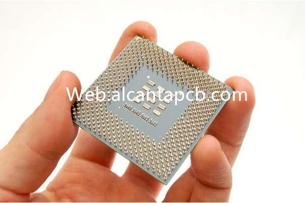
Eine KI-Beschleuniger-Leiterplatte ist eine Leiterplatte, die speziell für die Anforderungen von KI-Beschleunigern entwickelt wurde. KI-Beschleuniger sind spezielle Hardware zur Beschleunigung von KI-Berechnungen, einschließlich Deep Learning, maschinelles Lernen, und neuronale Netzwerkverarbeitung. Diese Beschleuniger werden in verschiedenen Anwendungen eingesetzt, wie Rechenzentren, autonome Fahrzeuge, Robotik, und Edge-Computing-Geräte.
Das Design von AI Accelerator Leiterplatten konzentriert sich auf die Optimierung der Energieeffizienz, Wärmemanagement, und Signalintegrität, um die hohen Leistungs- und geringen Latenzanforderungen von KI-Workloads zu erfüllen. KI-Beschleuniger-Leiterplatten enthalten häufig Verbindungen mit hoher Dichte, fortschrittliche Materialien, und mehrschichtige Konfigurationen, um den komplexen Schaltkreisen und der hohen Datenbandbreite gerecht zu werden, die von KI-Prozessoren benötigt werden.
AI Accelerator-PCBs müssen auch Hochgeschwindigkeitsschnittstellen unterstützen, wie PCIe, HBM (Speicher mit hoher Bandbreite), und NVLink, die für den schnellen Datentransfer zwischen dem KI-Beschleuniger und anderen Systemkomponenten unerlässlich sind. Die Integration dieser Schnittstellen, zusammen mit der Notwendigkeit einer effizienten Stromverteilung und eines Wärmemanagements, macht AI Accelerator-Leiterplatten zu den anspruchsvollsten und anspruchsvollsten Leiterplatten in der Entwicklung und Herstellung.
Materialien, die in KI-Beschleuniger-Leiterplatten verwendet werden
Die Wahl der Materialien für AI Accelerator PCBs ist entscheidend, um eine hohe Leistung sicherzustellen, Zuverlässigkeit, und Langlebigkeit in KI-Systemen. Die Materialien müssen hervorragende elektrische Eigenschaften bieten, Wärmeleitfähigkeit, und mechanische Stabilität. Zu den gängigen Materialien, die in AI Accelerator-PCBs verwendet werden, gehören::
AI Accelerator-Leiterplatten verwenden häufig Hochgeschwindigkeitslaminate wie Rogers, Isola, oder Taconic-Materialien, die eine niedrige Dielektrizitätskonstante bieten (Dk) und geringer Verlustfaktor (Df). Diese Materialien sind für die Minimierung von Signalverlusten und die Gewährleistung der Signalintegrität in Hochfrequenzschaltungen unerlässlich.
In KI-Beschleuniger-Leiterplatten werden dicke Kupferfolien verwendet, um den hohen Stromanforderungen von KI-Beschleunigern gerecht zu werden. Die Verwendung schwerer Kupferschichten sorgt für eine effiziente Stromverteilung und verringert das Risiko einer Überhitzung.
Aufgrund der hohen Leistungsdichte von KI-Prozessoren ist ein effektives Wärmemanagement für AI Accelerator-PCBs von entscheidender Bedeutung. Materialien mit hoher Wärmeleitfähigkeit, wie thermische Vias, Wärmeleitpads, und Kühlkörper, sind in das PCB-Design integriert, um die Wärme effizient abzuleiten.
AI Accelerator-Leiterplatten können auch fortschrittliche Substratmaterialien wie keramikbasierte Substrate oder Metallkern-Leiterplatten verwenden (MCPCBs) zur Verbesserung der thermischen Leistung und der mechanischen Festigkeit. Diese Materialien tragen dazu bei, die Integrität der Leiterplatte in Umgebungen mit hohen Temperaturen aufrechtzuerhalten.
HDI-Technologie wird häufig in AI Accelerator-Leiterplatten eingesetzt, um eine hohe Komponentendichte und komplexes Routing zu erreichen. Bei dieser Technologie kommen Microvias zum Einsatz, Blind- und Buried-Vias, und dünne dielektrische Schichten zur Herstellung mehrschichtiger Leiterplatten mit hoher Verbindungsdichte.
Die Auswahl der Materialien richtet sich nach den spezifischen Anforderungen der KI-Anwendung, einschließlich Verarbeitungsgeschwindigkeit, Stromverbrauch, Wärmemanagement, und Umweltfaktoren.
Designüberlegungen für KI-Beschleuniger-PCBs
Bei der Entwicklung von KI-Beschleuniger-Leiterplatten müssen mehrere wichtige Herausforderungen bewältigt werden, um optimale Leistung und Zuverlässigkeit sicherzustellen. Zu den entscheidenden Designüberlegungen gehören::
KI-Beschleuniger benötigen eine stabile und effiziente Stromversorgung, um komplexe Berechnungen durchzuführen. Das PCB-Design muss breite Leistungsebenen umfassen, Stromverteilungsnetze mit niedriger Induktivität (PDNs), und Entkopplungskondensatoren, um Spannungsschwankungen zu minimieren und die Stromintegrität sicherzustellen.
Eine schnelle Datenübertragung zwischen dem KI-Beschleuniger und anderen Komponenten ist entscheidend für die KI-Leistung. Das PCB-Design muss den Signalverlust minimieren, Übersprechen, und elektromagnetische Störungen (EMI) durch sorgfältiges Verlegen von Hochgeschwindigkeitsleitungen, unter Verwendung einer kontrollierten Impedanz, und Implementierung geeigneter Erdungstechniken.
KI-Beschleuniger erzeugen erhebliche Wärme, Dies kann die Leistung und Zuverlässigkeit beeinträchtigen, wenn es nicht ordnungsgemäß verwaltet wird. Das PCB-Design muss thermische Durchkontaktierungen enthalten, Kühlkörper, und Wärmeleitpads zur effizienten Wärmeableitung. Fortschrittliche Kühllösungen, wie Flüssigkeitskühlung oder Heatpipes, kann auch für leistungsstarke KI-Systeme erforderlich sein.
Die Platzierung von Komponenten auf der Leiterplatte und die Leiterbahnführung müssen optimiert werden, um Signalverzögerungen zu reduzieren, Lärm minimieren, und sorgen für eine effiziente Stromverteilung. Das Layout muss auch die mechanischen Einschränkungen der Leiterplatte berücksichtigen, wie zum Beispiel die Größe, Form, und Montageanforderungen.
KI-Beschleuniger-PCBs verfügen häufig über Hochgeschwindigkeitsschnittstellen, wie PCIe, HBM, und NVLink, die ein präzises Routing und Signalintegritätsmanagement erfordern. Das Design muss sicherstellen, dass diese Schnittstellen ihr maximales Potenzial ausschöpfen, ohne dass es zu Latenz oder Signalverschlechterung kommt.
KI-Beschleuniger-Leiterplatten verfügen in der Regel über mehrschichtige Aufbauten, um die komplexen Schaltkreise und hochdichten Verbindungen aufzunehmen, die für KI-Beschleuniger erforderlich sind. Das Stackup-Design muss die Signalintegrität ausgleichen, Machtintegrität, und Wärmemanagement bei gleichzeitiger Erfüllung der mechanischen und Umgebungsanforderungen der Anwendung.
Das Design von AI Accelerator-PCBs ist ein kollaborativer Prozess, der eine enge Abstimmung zwischen PCB-Designern erfordert, Elektroingenieure, Thermoingenieure, und Maschinenbauingenieure, um die gewünschte Leistung und Zuverlässigkeit zu erreichen.
Herstellungsprozess von KI-Beschleuniger-Leiterplatten
Der Herstellungsprozess von AI Accelerator PCBs umfasst mehrere Phasen, Jedes ist darauf ausgelegt, die Präzision und Qualität des Endprodukts sicherzustellen. Der Prozess umfasst:
Der Prozess beginnt mit der Auswahl der geeigneten Materialien, wie Hochgeschwindigkeitslaminate, Kupferfolien, und Wärmemanagementmaterialien. Diese Materialien werden dann zusammenlaminiert, um das PCB-Substrat zu bilden.
Mikrovias, Blind Vias, und Durchgangslöcher werden in die Leiterplatte gebohrt, um elektrische Verbindungen zwischen den verschiedenen Schichten herzustellen. Für Microvias wird häufig Laserbohren eingesetzt, während bei größeren Durchkontaktierungen mechanisches Bohren zum Einsatz kommt.
Das Schaltungsmuster wird mit einem fotolithografischen Verfahren auf die Leiterplatte übertragen. Auf die Oberfläche der Leiterplatte wird ein Fotolack aufgetragen, und das Schaltungsmuster wird mit UV-Licht belichtet. Anschließend werden die freigelegten Stellen weggeätzt, hinterlässt die gewünschten Kupferspuren.
Die Durchkontaktierungen und Durchgangslöcher werden mit Kupfer beschichtet, um elektrische Verbindungen zwischen den Schichten herzustellen. Anschließend wird die Leiterplatte mit einem Oberflächenfinish beschichtet, wie ENIG (Chemisches Nickel-Immersionsgold) oder OSP (Organisches Lötbarkeitskonservierungsmittel), um das Kupfer zu schützen und die Lötbarkeit zu verbessern.
Der KI-Beschleuniger und andere Komponenten werden mithilfe automatisierter Bestückungsautomaten auf der Leiterplatte platziert. Anschließend werden die Bauteile mittels Reflow-Löten oder Wellenlöten auf die Leiterplatte gelötet.
Die fertige Leiterplatte wird strengen Tests unterzogen, um sicherzustellen, dass sie den Designspezifikationen und Qualitätsstandards entspricht. Diese Prüfung umfasst elektrische Prüfungen, Signalintegritätsprüfung, thermische Prüfung, und Sichtprüfung.
Der Herstellungsprozess von KI-Beschleuniger-Leiterplatten erfordert Präzision und Liebe zum Detail, um sicherzustellen, dass das Endprodukt den hohen Leistungsanforderungen von KI-Anwendungen entspricht.
Anwendungen von KI-Beschleuniger-PCBs
KI-Beschleuniger-PCBs werden in einer Vielzahl von Anwendungen eingesetzt, bei denen hohe Rechenleistung und Effizienz erforderlich sind. Zu den wichtigsten Anwendungen gehören:
KI-Beschleuniger-PCBs werden in Rechenzentren zur Stromversorgung von KI-Servern und Hochleistungsrechnern eingesetzt (HPC) Systeme. Diese PCBs ermöglichen die Verarbeitung großer Datensätze und die Ausführung komplexer KI-Algorithmen in Echtzeit.
In autonomen Fahrzeugen, AI Accelerator PCBs werden zur Verarbeitung von Sensordaten verwendet, Führen Sie Entscheidungen in Echtzeit durch, und den Fahrzeugbetrieb steuern. Diese Leiterplatten sind für die Ermöglichung fortschrittlicher Fahrerassistenzsysteme von entscheidender Bedeutung (Adas) und autonome Fahrfunktionen.
AI Accelerator PCBs werden in der Robotik für Aufgaben wie die Objekterkennung eingesetzt, Wegplanung, und maschinelles Lernen. Diese Leiterplatten ermöglichen es Robotern, komplexe Aufgaben mit hoher Präzision und Effizienz auszuführen.
AI Accelerator PCBs werden in Edge-Computing-Geräten verwendet, um die KI-Verarbeitung näher an die Datenquelle zu bringen. Diese PCBs ermöglichen eine KI-Verarbeitung mit geringer Latenz in Anwendungen wie Smart-Kameras, IoT-Geräte, und industrielle Automatisierung.
Im Gesundheitswesen, AI Accelerator PCBs werden in der medizinischen Bildgebung eingesetzt, Diagnostik, und personalisierte Medizin. Diese PCBs ermöglichen die Verarbeitung großer Mengen medizinischer Daten und die Ausführung von KI-Algorithmen für eine genaue Diagnose und Behandlung.
Vorteile von AI Accelerator-PCBs
KI-Beschleuniger-Leiterplatten bieten mehrere Vorteile, die sie für fortgeschrittene KI-Anwendungen unverzichtbar machen:
KI-Beschleuniger-PCBs sind für die Bewältigung der hohen Rechenanforderungen von KI-Workloads konzipiert, ermöglicht eine schnelle und effiziente Verarbeitung komplexer Algorithmen.
Die fortschrittlichen Materialien und Designtechniken, die in AI Accelerator-PCBs verwendet werden, gewährleisten zuverlässige Leistung in anspruchsvollen Umgebungen, wie Rechenzentren und autonome Fahrzeuge.
AI Accelerator-PCBs bieten eine hervorragende Signalintegrität, Reduzierung des Risikos eines Signalverlusts, Lärm, und Störungen in Hochfrequenzkreisen.
AI Accelerator-PCBs enthalten fortschrittliche Wärmemanagementlösungen, um die Wärme effizient abzuleiten, Gewährleistung eines stabilen Betriebs auch bei hoher Leistungsbelastung.
FAQ
Was ist eine KI-Beschleunigerplatine??
Eine KI-Beschleuniger-Leiterplatte ist eine spezielle Leiterplatte, die zur Unterstützung der hohen Rechenanforderungen und Datenverarbeitungsaufgaben von KI-Beschleunigern entwickelt wurde, wie GPUs, TPUs, und benutzerdefinierte KI-Chips.
Welche Materialien werden in AI Accelerator PCBs verwendet??
AI Accelerator PCBs verwenden Hochgeschwindigkeitslaminatmaterialien, dicke Kupferfolien, Wärmemanagementmaterialien, und fortschrittliche Substrate, um eine hohe Leistung zu gewährleisten, Zuverlässigkeit, und thermische Effizienz.
Was sind die Designüberlegungen für AI Accelerator PCBs??
Zu den wichtigsten Designüberlegungen für AI Accelerator-PCBs gehört die Leistungsintegrität, Signalintegrität, Wärmemanagement, Platzierung der Komponenten, Hochgeschwindigkeitsschnittstellen, und mehrschichtiges Stapeldesign.
Wo werden KI-Beschleuniger-PCBs verwendet??
AI Accelerator PCBs werden in Rechenzentren eingesetzt, autonome Fahrzeuge, Robotik, Edge-Computing-Geräte, und Anwendungen im Gesundheitswesen, bei denen hohe Rechenleistung und Effizienz erforderlich sind.